{"title":"原位形成 SnSe2/SnSe 垂直异质结构,实现偏振可选带排列。","authors":"Rui Ge, Beituo Liu, Fengrui Sui, Yufan Zheng, Yilun Yu, Kaiqi Wang, Ruijuan Qi, Rong Huang, Fangyu Yue, Junhao Chu, Chun-Gang Duan","doi":"10.1002/smll.202404965","DOIUrl":null,"url":null,"abstract":"<p>2D van der Waals (vdW) layered semiconductor vertical heterostructures with controllable band alignment are highly desired for nanodevice applications including photodetection and photovoltaics. However, current 2D vdW heterostructures are mainly obtained via mechanical exfoliation and stacking process, intrinsically limiting the yield and reproducibility, hardly achieving large-area with specific orientation. Here, large-area vdW-epitaxial SnSe<sub>2</sub>/SnSe heterostructures are obtained by annealing layered SnSe. These in situ Raman analyses reveal the optimized annealing conditions for the phase transition of SnSe to SnSe<sub>2</sub>. The spherical aberration-corrected transmission electron microscopy investigations demonstrate that layered SnSe<sub>2</sub> epitaxially forms on SnSe surface with atomically sharp interface and specific orientation. Optical characterizations and theoretical calculations reveal valley polarization of the heterostructures that originate from SnSe, suggesting a naturally adjustable band alignment between type-II and type-III, only relying on the polarization angle of incident lights. This work not only offers a unique and accessible approach to obtaining large-area SnSe<sub>2</sub>/SnSe heterostructures with new insight into the formation mechanism of vdW heterostructures, but also opens the intriguing optical applications based on valleytronic nanoheterostructures.</p>","PeriodicalId":228,"journal":{"name":"Small","volume":"20 47","pages":""},"PeriodicalIF":12.1000,"publicationDate":"2024-08-18","publicationTypes":"Journal Article","fieldsOfStudy":null,"isOpenAccess":false,"openAccessPdf":"","citationCount":"0","resultStr":"{\"title\":\"In Situ Formation of SnSe2/SnSe Vertical Heterostructures toward Polarization Selectable Band Alignments\",\"authors\":\"Rui Ge, Beituo Liu, Fengrui Sui, Yufan Zheng, Yilun Yu, Kaiqi Wang, Ruijuan Qi, Rong Huang, Fangyu Yue, Junhao Chu, Chun-Gang Duan\",\"doi\":\"10.1002/smll.202404965\",\"DOIUrl\":null,\"url\":null,\"abstract\":\"<p>2D van der Waals (vdW) layered semiconductor vertical heterostructures with controllable band alignment are highly desired for nanodevice applications including photodetection and photovoltaics. However, current 2D vdW heterostructures are mainly obtained via mechanical exfoliation and stacking process, intrinsically limiting the yield and reproducibility, hardly achieving large-area with specific orientation. Here, large-area vdW-epitaxial SnSe<sub>2</sub>/SnSe heterostructures are obtained by annealing layered SnSe. These in situ Raman analyses reveal the optimized annealing conditions for the phase transition of SnSe to SnSe<sub>2</sub>. The spherical aberration-corrected transmission electron microscopy investigations demonstrate that layered SnSe<sub>2</sub> epitaxially forms on SnSe surface with atomically sharp interface and specific orientation. Optical characterizations and theoretical calculations reveal valley polarization of the heterostructures that originate from SnSe, suggesting a naturally adjustable band alignment between type-II and type-III, only relying on the polarization angle of incident lights. This work not only offers a unique and accessible approach to obtaining large-area SnSe<sub>2</sub>/SnSe heterostructures with new insight into the formation mechanism of vdW heterostructures, but also opens the intriguing optical applications based on valleytronic nanoheterostructures.</p>\",\"PeriodicalId\":228,\"journal\":{\"name\":\"Small\",\"volume\":\"20 47\",\"pages\":\"\"},\"PeriodicalIF\":12.1000,\"publicationDate\":\"2024-08-18\",\"publicationTypes\":\"Journal Article\",\"fieldsOfStudy\":null,\"isOpenAccess\":false,\"openAccessPdf\":\"\",\"citationCount\":\"0\",\"resultStr\":null,\"platform\":\"Semanticscholar\",\"paperid\":null,\"PeriodicalName\":\"Small\",\"FirstCategoryId\":\"88\",\"ListUrlMain\":\"https://onlinelibrary.wiley.com/doi/10.1002/smll.202404965\",\"RegionNum\":2,\"RegionCategory\":\"材料科学\",\"ArticlePicture\":[],\"TitleCN\":null,\"AbstractTextCN\":null,\"PMCID\":null,\"EPubDate\":\"\",\"PubModel\":\"\",\"JCR\":\"Q1\",\"JCRName\":\"CHEMISTRY, MULTIDISCIPLINARY\",\"Score\":null,\"Total\":0}","platform":"Semanticscholar","paperid":null,"PeriodicalName":"Small","FirstCategoryId":"88","ListUrlMain":"https://onlinelibrary.wiley.com/doi/10.1002/smll.202404965","RegionNum":2,"RegionCategory":"材料科学","ArticlePicture":[],"TitleCN":null,"AbstractTextCN":null,"PMCID":null,"EPubDate":"","PubModel":"","JCR":"Q1","JCRName":"CHEMISTRY, MULTIDISCIPLINARY","Score":null,"Total":0}
In Situ Formation of SnSe2/SnSe Vertical Heterostructures toward Polarization Selectable Band Alignments
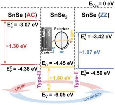
2D van der Waals (vdW) layered semiconductor vertical heterostructures with controllable band alignment are highly desired for nanodevice applications including photodetection and photovoltaics. However, current 2D vdW heterostructures are mainly obtained via mechanical exfoliation and stacking process, intrinsically limiting the yield and reproducibility, hardly achieving large-area with specific orientation. Here, large-area vdW-epitaxial SnSe2/SnSe heterostructures are obtained by annealing layered SnSe. These in situ Raman analyses reveal the optimized annealing conditions for the phase transition of SnSe to SnSe2. The spherical aberration-corrected transmission electron microscopy investigations demonstrate that layered SnSe2 epitaxially forms on SnSe surface with atomically sharp interface and specific orientation. Optical characterizations and theoretical calculations reveal valley polarization of the heterostructures that originate from SnSe, suggesting a naturally adjustable band alignment between type-II and type-III, only relying on the polarization angle of incident lights. This work not only offers a unique and accessible approach to obtaining large-area SnSe2/SnSe heterostructures with new insight into the formation mechanism of vdW heterostructures, but also opens the intriguing optical applications based on valleytronic nanoheterostructures.
期刊介绍:
Small serves as an exceptional platform for both experimental and theoretical studies in fundamental and applied interdisciplinary research at the nano- and microscale. The journal offers a compelling mix of peer-reviewed Research Articles, Reviews, Perspectives, and Comments.
With a remarkable 2022 Journal Impact Factor of 13.3 (Journal Citation Reports from Clarivate Analytics, 2023), Small remains among the top multidisciplinary journals, covering a wide range of topics at the interface of materials science, chemistry, physics, engineering, medicine, and biology.
Small's readership includes biochemists, biologists, biomedical scientists, chemists, engineers, information technologists, materials scientists, physicists, and theoreticians alike.
 求助内容:
求助内容: 应助结果提醒方式:


