Kimiyoshi Ichikawa, Tsubasa Matsumoto, Takao Inokuma, Satoshi Yamasaki, Christoph E. Nebel, Norio Tokuda
{"title":"面向晶圆制造、原子控制表面和低电阻率的金刚石同位外延生长技术","authors":"Kimiyoshi Ichikawa, Tsubasa Matsumoto, Takao Inokuma, Satoshi Yamasaki, Christoph E. Nebel, Norio Tokuda","doi":"10.1021/accountsmr.4c00123","DOIUrl":null,"url":null,"abstract":"Strong covalent bonds provide diamond with superior properties such as higher thermal conductivity, electron/hole mobilities, and wider bandgap than those of other semiconductors. This makes diamonds promising for next-generation power devices, optoelectronics, quantum technologies, and sensors. However, there are still challenges in realizing practical diamond electronic applications. Key issues include controlling the microwave plasma chemical vapor deposition (MPCVD) growth process to achieve a large size, smooth surfaces, and desired conductivity. Standard semiconductor processing techniques like polishing and ion implantation also need improvement for diamonds. This Account outlines three MPCVD growth technologies being investigated at Kanazawa University to address these challenges.","PeriodicalId":72040,"journal":{"name":"Accounts of materials research","volume":"26 1","pages":""},"PeriodicalIF":14.0000,"publicationDate":"2024-08-13","publicationTypes":"Journal Article","fieldsOfStudy":null,"isOpenAccess":false,"openAccessPdf":"","citationCount":"0","resultStr":"{\"title\":\"Diamond Homoepitaxial Growth Technology toward Wafer Fabrication, Atomically Controlled Surfaces, and Low Resistivity\",\"authors\":\"Kimiyoshi Ichikawa, Tsubasa Matsumoto, Takao Inokuma, Satoshi Yamasaki, Christoph E. Nebel, Norio Tokuda\",\"doi\":\"10.1021/accountsmr.4c00123\",\"DOIUrl\":null,\"url\":null,\"abstract\":\"Strong covalent bonds provide diamond with superior properties such as higher thermal conductivity, electron/hole mobilities, and wider bandgap than those of other semiconductors. This makes diamonds promising for next-generation power devices, optoelectronics, quantum technologies, and sensors. However, there are still challenges in realizing practical diamond electronic applications. Key issues include controlling the microwave plasma chemical vapor deposition (MPCVD) growth process to achieve a large size, smooth surfaces, and desired conductivity. Standard semiconductor processing techniques like polishing and ion implantation also need improvement for diamonds. This Account outlines three MPCVD growth technologies being investigated at Kanazawa University to address these challenges.\",\"PeriodicalId\":72040,\"journal\":{\"name\":\"Accounts of materials research\",\"volume\":\"26 1\",\"pages\":\"\"},\"PeriodicalIF\":14.0000,\"publicationDate\":\"2024-08-13\",\"publicationTypes\":\"Journal Article\",\"fieldsOfStudy\":null,\"isOpenAccess\":false,\"openAccessPdf\":\"\",\"citationCount\":\"0\",\"resultStr\":null,\"platform\":\"Semanticscholar\",\"paperid\":null,\"PeriodicalName\":\"Accounts of materials research\",\"FirstCategoryId\":\"1085\",\"ListUrlMain\":\"https://doi.org/10.1021/accountsmr.4c00123\",\"RegionNum\":0,\"RegionCategory\":null,\"ArticlePicture\":[],\"TitleCN\":null,\"AbstractTextCN\":null,\"PMCID\":null,\"EPubDate\":\"\",\"PubModel\":\"\",\"JCR\":\"Q1\",\"JCRName\":\"CHEMISTRY, MULTIDISCIPLINARY\",\"Score\":null,\"Total\":0}","platform":"Semanticscholar","paperid":null,"PeriodicalName":"Accounts of materials research","FirstCategoryId":"1085","ListUrlMain":"https://doi.org/10.1021/accountsmr.4c00123","RegionNum":0,"RegionCategory":null,"ArticlePicture":[],"TitleCN":null,"AbstractTextCN":null,"PMCID":null,"EPubDate":"","PubModel":"","JCR":"Q1","JCRName":"CHEMISTRY, MULTIDISCIPLINARY","Score":null,"Total":0}
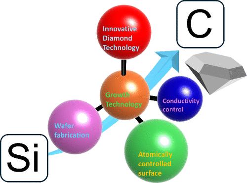
Strong covalent bonds provide diamond with superior properties such as higher thermal conductivity, electron/hole mobilities, and wider bandgap than those of other semiconductors. This makes diamonds promising for next-generation power devices, optoelectronics, quantum technologies, and sensors. However, there are still challenges in realizing practical diamond electronic applications. Key issues include controlling the microwave plasma chemical vapor deposition (MPCVD) growth process to achieve a large size, smooth surfaces, and desired conductivity. Standard semiconductor processing techniques like polishing and ion implantation also need improvement for diamonds. This Account outlines three MPCVD growth technologies being investigated at Kanazawa University to address these challenges.
 求助内容:
求助内容: 应助结果提醒方式:


