{"title":"用于超快二维闪存的可扩展集成工艺","authors":"Yongbo Jiang, Chunsen Liu, Zhenyuan Cao, Chuhang Li, Zizheng Liu, Chong Wang, Yutong Xiang, Peng Zhou","doi":"10.1038/s41928-024-01229-6","DOIUrl":null,"url":null,"abstract":"Data-driven computing is highly dependent on memory performance. Flash memory is presently the dominant non-volatile memory technology but suffers from limitations in terms of speed. Two-dimensional (2D) materials could potentially be used to create ultrafast flash memory. However, due to interface engineering problems, ultrafast non-volatile performance is presently restricted to exfoliated 2D materials, and there is a lack of performance demonstrations with short-channel devices. Here, we report a scalable integration process for ultrafast 2D flash memory that can be used to integrate 1,024 flash-memory devices with a yield of over 98%. We illustrate the approach with two different tunnelling barrier configurations of the memory stack (HfO2/Pt/HfO2 and Al2O3/Pt/Al2O3) and using transferred chemical vapour deposition-grown monolayer molybdenum disulfide. We also show that the channel length of the ultrafast flash memory can be scaled down to sub-10 nm, which is below the physical limit of silicon flash memory. Our sub-10 nm devices offer non-volatile information storage (up to 4 bits) and robust endurance (over 105). A scalable integration process for ultrafast two-dimensional flash memory can be used to integrate 1,024 devices with a yield of over 98%. The channel length of the devices could also be scaled down to sub-10 nm.","PeriodicalId":19064,"journal":{"name":"Nature Electronics","volume":"7 10","pages":"868-875"},"PeriodicalIF":33.7000,"publicationDate":"2024-08-12","publicationTypes":"Journal Article","fieldsOfStudy":null,"isOpenAccess":false,"openAccessPdf":"","citationCount":"0","resultStr":"{\"title\":\"A scalable integration process for ultrafast two-dimensional flash memory\",\"authors\":\"Yongbo Jiang, Chunsen Liu, Zhenyuan Cao, Chuhang Li, Zizheng Liu, Chong Wang, Yutong Xiang, Peng Zhou\",\"doi\":\"10.1038/s41928-024-01229-6\",\"DOIUrl\":null,\"url\":null,\"abstract\":\"Data-driven computing is highly dependent on memory performance. Flash memory is presently the dominant non-volatile memory technology but suffers from limitations in terms of speed. Two-dimensional (2D) materials could potentially be used to create ultrafast flash memory. However, due to interface engineering problems, ultrafast non-volatile performance is presently restricted to exfoliated 2D materials, and there is a lack of performance demonstrations with short-channel devices. Here, we report a scalable integration process for ultrafast 2D flash memory that can be used to integrate 1,024 flash-memory devices with a yield of over 98%. We illustrate the approach with two different tunnelling barrier configurations of the memory stack (HfO2/Pt/HfO2 and Al2O3/Pt/Al2O3) and using transferred chemical vapour deposition-grown monolayer molybdenum disulfide. We also show that the channel length of the ultrafast flash memory can be scaled down to sub-10 nm, which is below the physical limit of silicon flash memory. Our sub-10 nm devices offer non-volatile information storage (up to 4 bits) and robust endurance (over 105). A scalable integration process for ultrafast two-dimensional flash memory can be used to integrate 1,024 devices with a yield of over 98%. The channel length of the devices could also be scaled down to sub-10 nm.\",\"PeriodicalId\":19064,\"journal\":{\"name\":\"Nature Electronics\",\"volume\":\"7 10\",\"pages\":\"868-875\"},\"PeriodicalIF\":33.7000,\"publicationDate\":\"2024-08-12\",\"publicationTypes\":\"Journal Article\",\"fieldsOfStudy\":null,\"isOpenAccess\":false,\"openAccessPdf\":\"\",\"citationCount\":\"0\",\"resultStr\":null,\"platform\":\"Semanticscholar\",\"paperid\":null,\"PeriodicalName\":\"Nature Electronics\",\"FirstCategoryId\":\"5\",\"ListUrlMain\":\"https://www.nature.com/articles/s41928-024-01229-6\",\"RegionNum\":1,\"RegionCategory\":\"工程技术\",\"ArticlePicture\":[],\"TitleCN\":null,\"AbstractTextCN\":null,\"PMCID\":null,\"EPubDate\":\"\",\"PubModel\":\"\",\"JCR\":\"Q1\",\"JCRName\":\"ENGINEERING, ELECTRICAL & ELECTRONIC\",\"Score\":null,\"Total\":0}","platform":"Semanticscholar","paperid":null,"PeriodicalName":"Nature Electronics","FirstCategoryId":"5","ListUrlMain":"https://www.nature.com/articles/s41928-024-01229-6","RegionNum":1,"RegionCategory":"工程技术","ArticlePicture":[],"TitleCN":null,"AbstractTextCN":null,"PMCID":null,"EPubDate":"","PubModel":"","JCR":"Q1","JCRName":"ENGINEERING, ELECTRICAL & ELECTRONIC","Score":null,"Total":0}
A scalable integration process for ultrafast two-dimensional flash memory
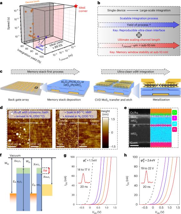
Data-driven computing is highly dependent on memory performance. Flash memory is presently the dominant non-volatile memory technology but suffers from limitations in terms of speed. Two-dimensional (2D) materials could potentially be used to create ultrafast flash memory. However, due to interface engineering problems, ultrafast non-volatile performance is presently restricted to exfoliated 2D materials, and there is a lack of performance demonstrations with short-channel devices. Here, we report a scalable integration process for ultrafast 2D flash memory that can be used to integrate 1,024 flash-memory devices with a yield of over 98%. We illustrate the approach with two different tunnelling barrier configurations of the memory stack (HfO2/Pt/HfO2 and Al2O3/Pt/Al2O3) and using transferred chemical vapour deposition-grown monolayer molybdenum disulfide. We also show that the channel length of the ultrafast flash memory can be scaled down to sub-10 nm, which is below the physical limit of silicon flash memory. Our sub-10 nm devices offer non-volatile information storage (up to 4 bits) and robust endurance (over 105). A scalable integration process for ultrafast two-dimensional flash memory can be used to integrate 1,024 devices with a yield of over 98%. The channel length of the devices could also be scaled down to sub-10 nm.
期刊介绍:
Nature Electronics is a comprehensive journal that publishes both fundamental and applied research in the field of electronics. It encompasses a wide range of topics, including the study of new phenomena and devices, the design and construction of electronic circuits, and the practical applications of electronics. In addition, the journal explores the commercial and industrial aspects of electronics research.
The primary focus of Nature Electronics is on the development of technology and its potential impact on society. The journal incorporates the contributions of scientists, engineers, and industry professionals, offering a platform for their research findings. Moreover, Nature Electronics provides insightful commentary, thorough reviews, and analysis of the key issues that shape the field, as well as the technologies that are reshaping society.
Like all journals within the prestigious Nature brand, Nature Electronics upholds the highest standards of quality. It maintains a dedicated team of professional editors and follows a fair and rigorous peer-review process. The journal also ensures impeccable copy-editing and production, enabling swift publication. Additionally, Nature Electronics prides itself on its editorial independence, ensuring unbiased and impartial reporting.
In summary, Nature Electronics is a leading journal that publishes cutting-edge research in electronics. With its multidisciplinary approach and commitment to excellence, the journal serves as a valuable resource for scientists, engineers, and industry professionals seeking to stay at the forefront of advancements in the field.