Chua-Chin Wang, L S S Pavan Kumar Chodisetti, Bo-Hao Liao, Pradyumna Vellanki, Tzung-Je Lee
{"title":"采用粗微调 VCO 和改进型 DQFD 的 1-6.5 Gbps 双环 CDR 设计","authors":"Chua-Chin Wang, L S S Pavan Kumar Chodisetti, Bo-Hao Liao, Pradyumna Vellanki, Tzung-Je Lee","doi":"10.1016/j.mejo.2024.106355","DOIUrl":null,"url":null,"abstract":"<div><p>A dual-loop CDR (Clock and Data Recovery) is presented to recover digital data from 1 to 6.5 Gbps. The presented frequency acquisition technique is based on full rate clock architecture. By utilizing modified Digital Quadri-correlator Frequency Detector (DQFD) and Frequency Increment/Decrement Control circuit, the lock-in range is improved. Furthermore, the issue of state loss during wide frequency range detection is successfully mitigated. The inclusion of two control wires in the Coarse-fine Tuning VCO enables the utilization of separate loop filters in the dual loops, resulting in a more effective reduction of noise and jitter. Utilizing a 40-nm CMOS process, the presented CDR design has been implemented. The post-layout simulation results at 6.5 Gbps shows a P2P and root-mean-square jitter values are 17.1 ps and 5.79 ps, respectively, for the retimed data.</p></div>","PeriodicalId":49818,"journal":{"name":"Microelectronics Journal","volume":null,"pages":null},"PeriodicalIF":1.9000,"publicationDate":"2024-08-05","publicationTypes":"Journal Article","fieldsOfStudy":null,"isOpenAccess":false,"openAccessPdf":"","citationCount":"0","resultStr":"{\"title\":\"A 1–6.5 Gbps dual-loop CDR design with Coarse-fine Tuning VCO and modified DQFD\",\"authors\":\"Chua-Chin Wang, L S S Pavan Kumar Chodisetti, Bo-Hao Liao, Pradyumna Vellanki, Tzung-Je Lee\",\"doi\":\"10.1016/j.mejo.2024.106355\",\"DOIUrl\":null,\"url\":null,\"abstract\":\"<div><p>A dual-loop CDR (Clock and Data Recovery) is presented to recover digital data from 1 to 6.5 Gbps. The presented frequency acquisition technique is based on full rate clock architecture. By utilizing modified Digital Quadri-correlator Frequency Detector (DQFD) and Frequency Increment/Decrement Control circuit, the lock-in range is improved. Furthermore, the issue of state loss during wide frequency range detection is successfully mitigated. The inclusion of two control wires in the Coarse-fine Tuning VCO enables the utilization of separate loop filters in the dual loops, resulting in a more effective reduction of noise and jitter. Utilizing a 40-nm CMOS process, the presented CDR design has been implemented. The post-layout simulation results at 6.5 Gbps shows a P2P and root-mean-square jitter values are 17.1 ps and 5.79 ps, respectively, for the retimed data.</p></div>\",\"PeriodicalId\":49818,\"journal\":{\"name\":\"Microelectronics Journal\",\"volume\":null,\"pages\":null},\"PeriodicalIF\":1.9000,\"publicationDate\":\"2024-08-05\",\"publicationTypes\":\"Journal Article\",\"fieldsOfStudy\":null,\"isOpenAccess\":false,\"openAccessPdf\":\"\",\"citationCount\":\"0\",\"resultStr\":null,\"platform\":\"Semanticscholar\",\"paperid\":null,\"PeriodicalName\":\"Microelectronics Journal\",\"FirstCategoryId\":\"5\",\"ListUrlMain\":\"https://www.sciencedirect.com/science/article/pii/S1879239124000596\",\"RegionNum\":3,\"RegionCategory\":\"工程技术\",\"ArticlePicture\":[],\"TitleCN\":null,\"AbstractTextCN\":null,\"PMCID\":null,\"EPubDate\":\"\",\"PubModel\":\"\",\"JCR\":\"Q3\",\"JCRName\":\"ENGINEERING, ELECTRICAL & ELECTRONIC\",\"Score\":null,\"Total\":0}","platform":"Semanticscholar","paperid":null,"PeriodicalName":"Microelectronics Journal","FirstCategoryId":"5","ListUrlMain":"https://www.sciencedirect.com/science/article/pii/S1879239124000596","RegionNum":3,"RegionCategory":"工程技术","ArticlePicture":[],"TitleCN":null,"AbstractTextCN":null,"PMCID":null,"EPubDate":"","PubModel":"","JCR":"Q3","JCRName":"ENGINEERING, ELECTRICAL & ELECTRONIC","Score":null,"Total":0}
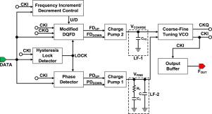
A 1–6.5 Gbps dual-loop CDR design with Coarse-fine Tuning VCO and modified DQFD
A dual-loop CDR (Clock and Data Recovery) is presented to recover digital data from 1 to 6.5 Gbps. The presented frequency acquisition technique is based on full rate clock architecture. By utilizing modified Digital Quadri-correlator Frequency Detector (DQFD) and Frequency Increment/Decrement Control circuit, the lock-in range is improved. Furthermore, the issue of state loss during wide frequency range detection is successfully mitigated. The inclusion of two control wires in the Coarse-fine Tuning VCO enables the utilization of separate loop filters in the dual loops, resulting in a more effective reduction of noise and jitter. Utilizing a 40-nm CMOS process, the presented CDR design has been implemented. The post-layout simulation results at 6.5 Gbps shows a P2P and root-mean-square jitter values are 17.1 ps and 5.79 ps, respectively, for the retimed data.
期刊介绍:
Published since 1969, the Microelectronics Journal is an international forum for the dissemination of research and applications of microelectronic systems, circuits, and emerging technologies. Papers published in the Microelectronics Journal have undergone peer review to ensure originality, relevance, and timeliness. The journal thus provides a worldwide, regular, and comprehensive update on microelectronic circuits and systems.
The Microelectronics Journal invites papers describing significant research and applications in all of the areas listed below. Comprehensive review/survey papers covering recent developments will also be considered. The Microelectronics Journal covers circuits and systems. This topic includes but is not limited to: Analog, digital, mixed, and RF circuits and related design methodologies; Logic, architectural, and system level synthesis; Testing, design for testability, built-in self-test; Area, power, and thermal analysis and design; Mixed-domain simulation and design; Embedded systems; Non-von Neumann computing and related technologies and circuits; Design and test of high complexity systems integration; SoC, NoC, SIP, and NIP design and test; 3-D integration design and analysis; Emerging device technologies and circuits, such as FinFETs, SETs, spintronics, SFQ, MTJ, etc.
Application aspects such as signal and image processing including circuits for cryptography, sensors, and actuators including sensor networks, reliability and quality issues, and economic models are also welcome.

 求助内容:
求助内容: 应助结果提醒方式:


