{"title":"氮化铝缓冲层厚度对 In0.17Al0.83N/GaN 高电子迁移率晶体管电子和电气特性的影响","authors":"Abdelmalek Douara, Abdelaziz Rabehi, Mawloud Guermoui, Rania Daha, Imad Eddine Tibermacine","doi":"10.1134/S1063783424600766","DOIUrl":null,"url":null,"abstract":"<p>In this paper, we delved into the intricacies of In<sub>0.17</sub>Al<sub>0.83</sub>N/GaN high-electron-mobility transistors (HEMTs) using a comprehensive simulation model and by Leveraging the capabilities of Nextnano simulation software. We extensively explored how different thicknesses of the AlN buffer layer impact electronic and electrical properties. Our study was centered on scrutinizing the density and mobility of the two-dimensional electron gas (2-DEG) within the In<sub>0.17</sub>Al<sub>0.83</sub>N/GaN HEMT structure. Aiming to understand how different AlN buffer layer thicknesses impact device performance. Our findings unveil a crucial relationship between AlN buffer layer thickness and critical performance metrics. Specifically, we observed significant trends in output current and transconductance, shedding light on the direct influence of AlN thickness on device behavior. Our simulations identified an optimal AlN thickness of 350 nm, demonstrating the highest output current and surpassing a transconductance peak of 510 mS/mm. Importantly, our computational predictions closely align with experimental observations, validating the reliability and accuracy of our simulation model. Through this meticulous analysis, we contribute valuable insights that can guide the design and optimization of In<sub>0.17</sub>Al<sub>0.83</sub>N/GaN HEMT, paving the way for improved device performance and functionality across various electronic applications. Our study underscores the importance of considering AlN buffer layer thickness in designing and engineering high-performance HEMTs, highlighting avenues for future research and development in semiconductor device technology.</p>","PeriodicalId":731,"journal":{"name":"Physics of the Solid State","volume":"66 6","pages":"157 - 164"},"PeriodicalIF":0.9000,"publicationDate":"2024-08-07","publicationTypes":"Journal Article","fieldsOfStudy":null,"isOpenAccess":false,"openAccessPdf":"","citationCount":"0","resultStr":"{\"title\":\"Impact of AlN Buffer Layer Thickness on Electronic and Electrical Characteristics of In0.17Al0.83N/GaN High-Electron-Mobility Transistor\",\"authors\":\"Abdelmalek Douara, Abdelaziz Rabehi, Mawloud Guermoui, Rania Daha, Imad Eddine Tibermacine\",\"doi\":\"10.1134/S1063783424600766\",\"DOIUrl\":null,\"url\":null,\"abstract\":\"<p>In this paper, we delved into the intricacies of In<sub>0.17</sub>Al<sub>0.83</sub>N/GaN high-electron-mobility transistors (HEMTs) using a comprehensive simulation model and by Leveraging the capabilities of Nextnano simulation software. We extensively explored how different thicknesses of the AlN buffer layer impact electronic and electrical properties. Our study was centered on scrutinizing the density and mobility of the two-dimensional electron gas (2-DEG) within the In<sub>0.17</sub>Al<sub>0.83</sub>N/GaN HEMT structure. Aiming to understand how different AlN buffer layer thicknesses impact device performance. Our findings unveil a crucial relationship between AlN buffer layer thickness and critical performance metrics. Specifically, we observed significant trends in output current and transconductance, shedding light on the direct influence of AlN thickness on device behavior. Our simulations identified an optimal AlN thickness of 350 nm, demonstrating the highest output current and surpassing a transconductance peak of 510 mS/mm. Importantly, our computational predictions closely align with experimental observations, validating the reliability and accuracy of our simulation model. Through this meticulous analysis, we contribute valuable insights that can guide the design and optimization of In<sub>0.17</sub>Al<sub>0.83</sub>N/GaN HEMT, paving the way for improved device performance and functionality across various electronic applications. Our study underscores the importance of considering AlN buffer layer thickness in designing and engineering high-performance HEMTs, highlighting avenues for future research and development in semiconductor device technology.</p>\",\"PeriodicalId\":731,\"journal\":{\"name\":\"Physics of the Solid State\",\"volume\":\"66 6\",\"pages\":\"157 - 164\"},\"PeriodicalIF\":0.9000,\"publicationDate\":\"2024-08-07\",\"publicationTypes\":\"Journal Article\",\"fieldsOfStudy\":null,\"isOpenAccess\":false,\"openAccessPdf\":\"\",\"citationCount\":\"0\",\"resultStr\":null,\"platform\":\"Semanticscholar\",\"paperid\":null,\"PeriodicalName\":\"Physics of the Solid State\",\"FirstCategoryId\":\"101\",\"ListUrlMain\":\"https://link.springer.com/article/10.1134/S1063783424600766\",\"RegionNum\":4,\"RegionCategory\":\"物理与天体物理\",\"ArticlePicture\":[],\"TitleCN\":null,\"AbstractTextCN\":null,\"PMCID\":null,\"EPubDate\":\"\",\"PubModel\":\"\",\"JCR\":\"Q4\",\"JCRName\":\"PHYSICS, CONDENSED MATTER\",\"Score\":null,\"Total\":0}","platform":"Semanticscholar","paperid":null,"PeriodicalName":"Physics of the Solid State","FirstCategoryId":"101","ListUrlMain":"https://link.springer.com/article/10.1134/S1063783424600766","RegionNum":4,"RegionCategory":"物理与天体物理","ArticlePicture":[],"TitleCN":null,"AbstractTextCN":null,"PMCID":null,"EPubDate":"","PubModel":"","JCR":"Q4","JCRName":"PHYSICS, CONDENSED MATTER","Score":null,"Total":0}
Impact of AlN Buffer Layer Thickness on Electronic and Electrical Characteristics of In0.17Al0.83N/GaN High-Electron-Mobility Transistor
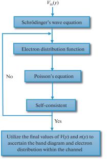
In this paper, we delved into the intricacies of In0.17Al0.83N/GaN high-electron-mobility transistors (HEMTs) using a comprehensive simulation model and by Leveraging the capabilities of Nextnano simulation software. We extensively explored how different thicknesses of the AlN buffer layer impact electronic and electrical properties. Our study was centered on scrutinizing the density and mobility of the two-dimensional electron gas (2-DEG) within the In0.17Al0.83N/GaN HEMT structure. Aiming to understand how different AlN buffer layer thicknesses impact device performance. Our findings unveil a crucial relationship between AlN buffer layer thickness and critical performance metrics. Specifically, we observed significant trends in output current and transconductance, shedding light on the direct influence of AlN thickness on device behavior. Our simulations identified an optimal AlN thickness of 350 nm, demonstrating the highest output current and surpassing a transconductance peak of 510 mS/mm. Importantly, our computational predictions closely align with experimental observations, validating the reliability and accuracy of our simulation model. Through this meticulous analysis, we contribute valuable insights that can guide the design and optimization of In0.17Al0.83N/GaN HEMT, paving the way for improved device performance and functionality across various electronic applications. Our study underscores the importance of considering AlN buffer layer thickness in designing and engineering high-performance HEMTs, highlighting avenues for future research and development in semiconductor device technology.
期刊介绍:
Presents the latest results from Russia’s leading researchers in condensed matter physics at the Russian Academy of Sciences and other prestigious institutions. Covers all areas of solid state physics including solid state optics, solid state acoustics, electronic and vibrational spectra, phase transitions, ferroelectricity, magnetism, and superconductivity. Also presents review papers on the most important problems in solid state physics.
 求助内容:
求助内容: 应助结果提醒方式:


