{"title":"从半导体带结构各向异性看电磁高波与 \"绝缘体-半导体-绝缘体 \"纳米结构的相互作用","authors":"I. A. Kuznetsova, O. V. Savenko","doi":"10.1134/S0030400X24020127","DOIUrl":null,"url":null,"abstract":"<p>The problem of electromagnetic H-wave interaction with a layered “insulator–semiconductor–insulator” nanostructure is solved. We assume that the semiconductor layer thickness can be comparable to or less than the charge carrier de Broglie wavelength. Charge carrier surface scattering is taken into account by the Soffer boundary conditions. The electromagnetic wave frequency is less than the plasma resonance frequency. The constant energy surface is an ellipsoid of revolution. Analytical expressions are obtained for the reflection, transmission and absorption coefficients. Calculations are performed for the limiting cases of a degenerate and nondegenerate electron gas. We analyze the dependences of the optical coefficients on dimensionless parameters: the semiconductor layer thickness, the electromagnetic wave frequency and incidence angle, the chemical potential, the ellipticity parameter, the insulating layer permittivities, and the “semiconductor–insulator” interface roughness parameters.</p>","PeriodicalId":723,"journal":{"name":"Optics and Spectroscopy","volume":"132 2","pages":"162 - 169"},"PeriodicalIF":0.9000,"publicationDate":"2024-08-07","publicationTypes":"Journal Article","fieldsOfStudy":null,"isOpenAccess":false,"openAccessPdf":"","citationCount":"0","resultStr":"{\"title\":\"Interaction of an Electromagnetic H-Wave with an “Insulator–Semiconductor–Insulator” Nanostructure in the View of Semiconductor Band Structure Anisotropy\",\"authors\":\"I. A. Kuznetsova, O. V. Savenko\",\"doi\":\"10.1134/S0030400X24020127\",\"DOIUrl\":null,\"url\":null,\"abstract\":\"<p>The problem of electromagnetic H-wave interaction with a layered “insulator–semiconductor–insulator” nanostructure is solved. We assume that the semiconductor layer thickness can be comparable to or less than the charge carrier de Broglie wavelength. Charge carrier surface scattering is taken into account by the Soffer boundary conditions. The electromagnetic wave frequency is less than the plasma resonance frequency. The constant energy surface is an ellipsoid of revolution. Analytical expressions are obtained for the reflection, transmission and absorption coefficients. Calculations are performed for the limiting cases of a degenerate and nondegenerate electron gas. We analyze the dependences of the optical coefficients on dimensionless parameters: the semiconductor layer thickness, the electromagnetic wave frequency and incidence angle, the chemical potential, the ellipticity parameter, the insulating layer permittivities, and the “semiconductor–insulator” interface roughness parameters.</p>\",\"PeriodicalId\":723,\"journal\":{\"name\":\"Optics and Spectroscopy\",\"volume\":\"132 2\",\"pages\":\"162 - 169\"},\"PeriodicalIF\":0.9000,\"publicationDate\":\"2024-08-07\",\"publicationTypes\":\"Journal Article\",\"fieldsOfStudy\":null,\"isOpenAccess\":false,\"openAccessPdf\":\"\",\"citationCount\":\"0\",\"resultStr\":null,\"platform\":\"Semanticscholar\",\"paperid\":null,\"PeriodicalName\":\"Optics and Spectroscopy\",\"FirstCategoryId\":\"101\",\"ListUrlMain\":\"https://link.springer.com/article/10.1134/S0030400X24020127\",\"RegionNum\":4,\"RegionCategory\":\"物理与天体物理\",\"ArticlePicture\":[],\"TitleCN\":null,\"AbstractTextCN\":null,\"PMCID\":null,\"EPubDate\":\"\",\"PubModel\":\"\",\"JCR\":\"Q4\",\"JCRName\":\"OPTICS\",\"Score\":null,\"Total\":0}","platform":"Semanticscholar","paperid":null,"PeriodicalName":"Optics and Spectroscopy","FirstCategoryId":"101","ListUrlMain":"https://link.springer.com/article/10.1134/S0030400X24020127","RegionNum":4,"RegionCategory":"物理与天体物理","ArticlePicture":[],"TitleCN":null,"AbstractTextCN":null,"PMCID":null,"EPubDate":"","PubModel":"","JCR":"Q4","JCRName":"OPTICS","Score":null,"Total":0}
引用次数: 0
摘要
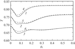
摘要 解决了电磁 H 波与层状 "绝缘体-半导体-绝缘体 "纳米结构的相互作用问题。我们假定半导体层的厚度可以与电荷载流子的德布罗格利波长相当或更小。索弗边界条件考虑了电荷载流子表面散射。电磁波频率小于等离子体共振频率。恒定能量面是一个旋转椭圆体。得到了反射、透射和吸收系数的分析表达式。对变性和非变性电子气体的极限情况进行了计算。我们分析了光学系数与无量纲参数的关系:半导体层厚度、电磁波频率和入射角、化学势、椭圆度参数、绝缘层介电常数以及 "半导体-绝缘体 "界面粗糙度参数。
Interaction of an Electromagnetic H-Wave with an “Insulator–Semiconductor–Insulator” Nanostructure in the View of Semiconductor Band Structure Anisotropy
The problem of electromagnetic H-wave interaction with a layered “insulator–semiconductor–insulator” nanostructure is solved. We assume that the semiconductor layer thickness can be comparable to or less than the charge carrier de Broglie wavelength. Charge carrier surface scattering is taken into account by the Soffer boundary conditions. The electromagnetic wave frequency is less than the plasma resonance frequency. The constant energy surface is an ellipsoid of revolution. Analytical expressions are obtained for the reflection, transmission and absorption coefficients. Calculations are performed for the limiting cases of a degenerate and nondegenerate electron gas. We analyze the dependences of the optical coefficients on dimensionless parameters: the semiconductor layer thickness, the electromagnetic wave frequency and incidence angle, the chemical potential, the ellipticity parameter, the insulating layer permittivities, and the “semiconductor–insulator” interface roughness parameters.
期刊介绍:
Optics and Spectroscopy (Optika i spektroskopiya), founded in 1956, presents original and review papers in various fields of modern optics and spectroscopy in the entire wavelength range from radio waves to X-rays. Topics covered include problems of theoretical and experimental spectroscopy of atoms, molecules, and condensed state, lasers and the interaction of laser radiation with matter, physical and geometrical optics, holography, and physical principles of optical instrument making.
 求助内容:
求助内容: 应助结果提醒方式:


