{"title":"用于晶圆级集成二维兼容高κ金属栅极的超扁平单晶六方氮化硼","authors":"Yani Wang, Chao Zhao, Xin Gao, Liming Zheng, Jun Qian, Xiaoyin Gao, Jiade Li, Junchuan Tang, Congwei Tan, Jiahao Wang, Xuetao Zhu, Jiandong Guo, Zhongfan Liu, Feng Ding, Hailin Peng","doi":"10.1038/s41563-024-01968-z","DOIUrl":null,"url":null,"abstract":"Hexagonal boron nitride (hBN) has emerged as a promising protection layer for dielectric integration in the next-generation large-scale integrated electronics. Although numerous efforts have been devoted to growing single-crystal hBN film, wafer-scale ultraflat hBN has still not been achieved. Here, we report the epitaxial growth of 4 in. ultraflat single-crystal hBN on Cu0.8Ni0.2(111)/sapphire wafers. The strong coupling between hBN and Cu0.8Ni0.2(111) suppresses the formation of wrinkles and ensures the seamless stitching of parallelly aligned hBN domains, resulting in an ultraflat single-crystal hBN film on a wafer scale. Using the ultraflat hBN as a protective layer, we integrate the wafer-scale ultrathin high-κ dielectrics onto two-dimensional (2D) materials with a damage-free interface. The obtained hBN/HfO2 composite dielectric exhibits an ultralow current leakage (2.36 × 10⁻⁶ A cm−2) and an ultrathin equivalent oxide thickness of 0.52 nm, which meets the targets of the International Roadmap for Devices and Systems. Our findings pave the way to the synthesis of ultraflat 2D materials and integration of future 2D electronics. The synthesis of wafer-scale ultraflat single-crystal hexagonal boron nitride film is realized by strong coupling to a Cu0.8Ni0.2(111)/sapphire wafer, providing a potential method for industry-compatible high-κ dielectric integration in two-dimensional electronics.","PeriodicalId":19058,"journal":{"name":"Nature Materials","volume":"23 11","pages":"1495-1501"},"PeriodicalIF":37.2000,"publicationDate":"2024-08-12","publicationTypes":"Journal Article","fieldsOfStudy":null,"isOpenAccess":false,"openAccessPdf":"","citationCount":"0","resultStr":"{\"title\":\"Ultraflat single-crystal hexagonal boron nitride for wafer-scale integration of a 2D-compatible high-κ metal gate\",\"authors\":\"Yani Wang, Chao Zhao, Xin Gao, Liming Zheng, Jun Qian, Xiaoyin Gao, Jiade Li, Junchuan Tang, Congwei Tan, Jiahao Wang, Xuetao Zhu, Jiandong Guo, Zhongfan Liu, Feng Ding, Hailin Peng\",\"doi\":\"10.1038/s41563-024-01968-z\",\"DOIUrl\":null,\"url\":null,\"abstract\":\"Hexagonal boron nitride (hBN) has emerged as a promising protection layer for dielectric integration in the next-generation large-scale integrated electronics. Although numerous efforts have been devoted to growing single-crystal hBN film, wafer-scale ultraflat hBN has still not been achieved. Here, we report the epitaxial growth of 4 in. ultraflat single-crystal hBN on Cu0.8Ni0.2(111)/sapphire wafers. The strong coupling between hBN and Cu0.8Ni0.2(111) suppresses the formation of wrinkles and ensures the seamless stitching of parallelly aligned hBN domains, resulting in an ultraflat single-crystal hBN film on a wafer scale. Using the ultraflat hBN as a protective layer, we integrate the wafer-scale ultrathin high-κ dielectrics onto two-dimensional (2D) materials with a damage-free interface. The obtained hBN/HfO2 composite dielectric exhibits an ultralow current leakage (2.36 × 10⁻⁶ A cm−2) and an ultrathin equivalent oxide thickness of 0.52 nm, which meets the targets of the International Roadmap for Devices and Systems. Our findings pave the way to the synthesis of ultraflat 2D materials and integration of future 2D electronics. The synthesis of wafer-scale ultraflat single-crystal hexagonal boron nitride film is realized by strong coupling to a Cu0.8Ni0.2(111)/sapphire wafer, providing a potential method for industry-compatible high-κ dielectric integration in two-dimensional electronics.\",\"PeriodicalId\":19058,\"journal\":{\"name\":\"Nature Materials\",\"volume\":\"23 11\",\"pages\":\"1495-1501\"},\"PeriodicalIF\":37.2000,\"publicationDate\":\"2024-08-12\",\"publicationTypes\":\"Journal Article\",\"fieldsOfStudy\":null,\"isOpenAccess\":false,\"openAccessPdf\":\"\",\"citationCount\":\"0\",\"resultStr\":null,\"platform\":\"Semanticscholar\",\"paperid\":null,\"PeriodicalName\":\"Nature Materials\",\"FirstCategoryId\":\"88\",\"ListUrlMain\":\"https://www.nature.com/articles/s41563-024-01968-z\",\"RegionNum\":1,\"RegionCategory\":\"材料科学\",\"ArticlePicture\":[],\"TitleCN\":null,\"AbstractTextCN\":null,\"PMCID\":null,\"EPubDate\":\"\",\"PubModel\":\"\",\"JCR\":\"Q1\",\"JCRName\":\"CHEMISTRY, PHYSICAL\",\"Score\":null,\"Total\":0}","platform":"Semanticscholar","paperid":null,"PeriodicalName":"Nature Materials","FirstCategoryId":"88","ListUrlMain":"https://www.nature.com/articles/s41563-024-01968-z","RegionNum":1,"RegionCategory":"材料科学","ArticlePicture":[],"TitleCN":null,"AbstractTextCN":null,"PMCID":null,"EPubDate":"","PubModel":"","JCR":"Q1","JCRName":"CHEMISTRY, PHYSICAL","Score":null,"Total":0}
Ultraflat single-crystal hexagonal boron nitride for wafer-scale integration of a 2D-compatible high-κ metal gate
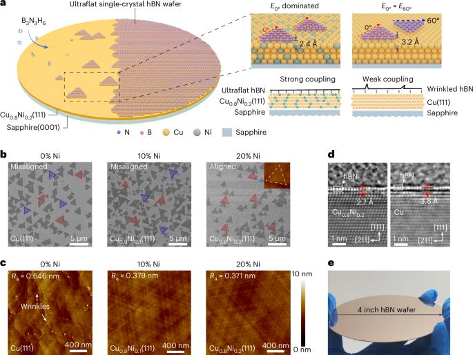
Hexagonal boron nitride (hBN) has emerged as a promising protection layer for dielectric integration in the next-generation large-scale integrated electronics. Although numerous efforts have been devoted to growing single-crystal hBN film, wafer-scale ultraflat hBN has still not been achieved. Here, we report the epitaxial growth of 4 in. ultraflat single-crystal hBN on Cu0.8Ni0.2(111)/sapphire wafers. The strong coupling between hBN and Cu0.8Ni0.2(111) suppresses the formation of wrinkles and ensures the seamless stitching of parallelly aligned hBN domains, resulting in an ultraflat single-crystal hBN film on a wafer scale. Using the ultraflat hBN as a protective layer, we integrate the wafer-scale ultrathin high-κ dielectrics onto two-dimensional (2D) materials with a damage-free interface. The obtained hBN/HfO2 composite dielectric exhibits an ultralow current leakage (2.36 × 10⁻⁶ A cm−2) and an ultrathin equivalent oxide thickness of 0.52 nm, which meets the targets of the International Roadmap for Devices and Systems. Our findings pave the way to the synthesis of ultraflat 2D materials and integration of future 2D electronics. The synthesis of wafer-scale ultraflat single-crystal hexagonal boron nitride film is realized by strong coupling to a Cu0.8Ni0.2(111)/sapphire wafer, providing a potential method for industry-compatible high-κ dielectric integration in two-dimensional electronics.
期刊介绍:
Nature Materials is a monthly multi-disciplinary journal aimed at bringing together cutting-edge research across the entire spectrum of materials science and engineering. It covers all applied and fundamental aspects of the synthesis/processing, structure/composition, properties, and performance of materials. The journal recognizes that materials research has an increasing impact on classical disciplines such as physics, chemistry, and biology.
Additionally, Nature Materials provides a forum for the development of a common identity among materials scientists and encourages interdisciplinary collaboration. It takes an integrated and balanced approach to all areas of materials research, fostering the exchange of ideas between scientists involved in different disciplines.
Nature Materials is an invaluable resource for scientists in academia and industry who are active in discovering and developing materials and materials-related concepts. It offers engaging and informative papers of exceptional significance and quality, with the aim of influencing the development of society in the future.