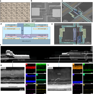
互补二维场效应晶体管的单片三维集成。

IF 38.1 1区 材料科学 Q1 MATERIALS SCIENCE, MULTIDISCIPLINARY
Rahul Pendurthi, Najam U Sakib, Muhtasim Ul Karim Sadaf, Zhiyu Zhang, Yongwen Sun, Chen Chen, Darsith Jayachandran, Aaryan Oberoi, Subir Ghosh, Shalini Kumari, Sergei P. Stepanoff, Divya Somvanshi, Yang Yang, Joan M. Redwing, Douglas E. Wolfe, Saptarshi Das
{"title":"互补二维场效应晶体管的单片三维集成。","authors":"Rahul Pendurthi, Najam U Sakib, Muhtasim Ul Karim Sadaf, Zhiyu Zhang, Yongwen Sun, Chen Chen, Darsith Jayachandran, Aaryan Oberoi, Subir Ghosh, Shalini Kumari, Sergei P. Stepanoff, Divya Somvanshi, Yang Yang, Joan M. Redwing, Douglas E. Wolfe, Saptarshi Das","doi":"10.1038/s41565-024-01705-2","DOIUrl":null,"url":null,"abstract":"The semiconductor industry is transitioning to the ‘More Moore’ era, driven by the adoption of three-dimensional (3D) integration schemes surpassing the limitations of traditional two-dimensional scaling. Although innovative packaging solutions have made 3D integrated circuits (ICs) commercially viable, the inclusion of through-silicon vias and microbumps brings about increased area overhead and introduces parasitic capacitances that limit overall performance. Monolithic 3D integration (M3D) is regarded as the future of 3D ICs, yet its application faces hurdles in silicon ICs due to restricted thermal processing budgets in upper tiers, which can degrade device performance. To overcome these limitations, emerging materials like carbon nanotubes and two-dimensional semiconductors have been integrated into the back end of silicon ICs. Here we report the M3D integration of complementary WSe2 FETs, in which n-type FETs are placed in tier 1 and p-type FETs are placed in tier 2. In particular, we achieve dense and scaled integration through 300 nm vias with a pitch of <1 µm, connecting more than 300 devices in tiers 1 and 2. Moreover, we have effectively implemented vertically integrated logic gates, encompassing inverters, NAND gates and NOR gates. Our demonstration highlights the two-dimensional materials’ role in advancing M3D integration in complementary metal–oxide–semiconductor circuits. Monolithic 3D integration of complementary WSe2 FETs has been achieved, featuring n-type FETs in tier 1 and p-type FETs in tier 2. Dense vias are realized using a pitch of less than 1 µm, facilitating 3D inverters as well as NAND and NOR logic functionalities.","PeriodicalId":18915,"journal":{"name":"Nature nanotechnology","volume":"19 7","pages":"970-977"},"PeriodicalIF":38.1000,"publicationDate":"2024-07-23","publicationTypes":"Journal Article","fieldsOfStudy":null,"isOpenAccess":false,"openAccessPdf":"","citationCount":"0","resultStr":"{\"title\":\"Monolithic three-dimensional integration of complementary two-dimensional field-effect transistors\",\"authors\":\"Rahul Pendurthi, Najam U Sakib, Muhtasim Ul Karim Sadaf, Zhiyu Zhang, Yongwen Sun, Chen Chen, Darsith Jayachandran, Aaryan Oberoi, Subir Ghosh, Shalini Kumari, Sergei P. Stepanoff, Divya Somvanshi, Yang Yang, Joan M. Redwing, Douglas E. Wolfe, Saptarshi Das\",\"doi\":\"10.1038/s41565-024-01705-2\",\"DOIUrl\":null,\"url\":null,\"abstract\":\"The semiconductor industry is transitioning to the ‘More Moore’ era, driven by the adoption of three-dimensional (3D) integration schemes surpassing the limitations of traditional two-dimensional scaling. Although innovative packaging solutions have made 3D integrated circuits (ICs) commercially viable, the inclusion of through-silicon vias and microbumps brings about increased area overhead and introduces parasitic capacitances that limit overall performance. Monolithic 3D integration (M3D) is regarded as the future of 3D ICs, yet its application faces hurdles in silicon ICs due to restricted thermal processing budgets in upper tiers, which can degrade device performance. To overcome these limitations, emerging materials like carbon nanotubes and two-dimensional semiconductors have been integrated into the back end of silicon ICs. Here we report the M3D integration of complementary WSe2 FETs, in which n-type FETs are placed in tier 1 and p-type FETs are placed in tier 2. In particular, we achieve dense and scaled integration through 300 nm vias with a pitch of <1 µm, connecting more than 300 devices in tiers 1 and 2. Moreover, we have effectively implemented vertically integrated logic gates, encompassing inverters, NAND gates and NOR gates. Our demonstration highlights the two-dimensional materials’ role in advancing M3D integration in complementary metal–oxide–semiconductor circuits. Monolithic 3D integration of complementary WSe2 FETs has been achieved, featuring n-type FETs in tier 1 and p-type FETs in tier 2. Dense vias are realized using a pitch of less than 1 µm, facilitating 3D inverters as well as NAND and NOR logic functionalities.\",\"PeriodicalId\":18915,\"journal\":{\"name\":\"Nature nanotechnology\",\"volume\":\"19 7\",\"pages\":\"970-977\"},\"PeriodicalIF\":38.1000,\"publicationDate\":\"2024-07-23\",\"publicationTypes\":\"Journal Article\",\"fieldsOfStudy\":null,\"isOpenAccess\":false,\"openAccessPdf\":\"\",\"citationCount\":\"0\",\"resultStr\":null,\"platform\":\"Semanticscholar\",\"paperid\":null,\"PeriodicalName\":\"Nature nanotechnology\",\"FirstCategoryId\":\"88\",\"ListUrlMain\":\"https://www.nature.com/articles/s41565-024-01705-2\",\"RegionNum\":1,\"RegionCategory\":\"材料科学\",\"ArticlePicture\":[],\"TitleCN\":null,\"AbstractTextCN\":null,\"PMCID\":null,\"EPubDate\":\"\",\"PubModel\":\"\",\"JCR\":\"Q1\",\"JCRName\":\"MATERIALS SCIENCE, MULTIDISCIPLINARY\",\"Score\":null,\"Total\":0}","platform":"Semanticscholar","paperid":null,"PeriodicalName":"Nature nanotechnology","FirstCategoryId":"88","ListUrlMain":"https://www.nature.com/articles/s41565-024-01705-2","RegionNum":1,"RegionCategory":"材料科学","ArticlePicture":[],"TitleCN":null,"AbstractTextCN":null,"PMCID":null,"EPubDate":"","PubModel":"","JCR":"Q1","JCRName":"MATERIALS SCIENCE, MULTIDISCIPLINARY","Score":null,"Total":0}
引用次数: 0

摘要

在三维(3D)集成方案的推动下,半导体行业正在向 "更摩尔"(More Moore)时代过渡,超越了传统二维扩展的局限性。虽然创新的封装解决方案使三维集成电路(IC)具有了商业可行性,但硅通孔和微凸块的加入增加了面积开销,并引入了限制整体性能的寄生电容。单片三维集成(M3D)被认为是三维集成电路的未来发展方向,但在硅集成电路中的应用却面临着障碍,因为上层的热处理预算有限,会降低器件性能。为了克服这些限制,碳纳米管和二维半导体等新兴材料已被集成到硅集成电路的后端。在此,我们报告了互补 WSe2 FET 的 M3D 集成,其中 n 型 FET 位于第 1 层,p 型 FET 位于第 2 层。特别是,我们通过间距为 300 nm 的通孔实现了高密度和按比例的集成。
本文章由计算机程序翻译,如有差异,请以英文原文为准。

Monolithic three-dimensional integration of complementary two-dimensional field-effect transistors

Monolithic three-dimensional integration of complementary two-dimensional field-effect transistors

Monolithic three-dimensional integration of complementary two-dimensional field-effect transistors
The semiconductor industry is transitioning to the ‘More Moore’ era, driven by the adoption of three-dimensional (3D) integration schemes surpassing the limitations of traditional two-dimensional scaling. Although innovative packaging solutions have made 3D integrated circuits (ICs) commercially viable, the inclusion of through-silicon vias and microbumps brings about increased area overhead and introduces parasitic capacitances that limit overall performance. Monolithic 3D integration (M3D) is regarded as the future of 3D ICs, yet its application faces hurdles in silicon ICs due to restricted thermal processing budgets in upper tiers, which can degrade device performance. To overcome these limitations, emerging materials like carbon nanotubes and two-dimensional semiconductors have been integrated into the back end of silicon ICs. Here we report the M3D integration of complementary WSe2 FETs, in which n-type FETs are placed in tier 1 and p-type FETs are placed in tier 2. In particular, we achieve dense and scaled integration through 300 nm vias with a pitch of <1 µm, connecting more than 300 devices in tiers 1 and 2. Moreover, we have effectively implemented vertically integrated logic gates, encompassing inverters, NAND gates and NOR gates. Our demonstration highlights the two-dimensional materials’ role in advancing M3D integration in complementary metal–oxide–semiconductor circuits. Monolithic 3D integration of complementary WSe2 FETs has been achieved, featuring n-type FETs in tier 1 and p-type FETs in tier 2. Dense vias are realized using a pitch of less than 1 µm, facilitating 3D inverters as well as NAND and NOR logic functionalities.
求助全文
通过发布文献求助,成功后即可免费获取论文全文。 去求助
来源期刊
Nature nanotechnology
Nature nanotechnology 工程技术-材料科学:综合
CiteScore
59.70
自引率
0.80%
发文量
196
审稿时长
4-8 weeks
期刊介绍: Nature Nanotechnology is a prestigious journal that publishes high-quality papers in various areas of nanoscience and nanotechnology. The journal focuses on the design, characterization, and production of structures, devices, and systems that manipulate and control materials at atomic, molecular, and macromolecular scales. It encompasses both bottom-up and top-down approaches, as well as their combinations. Furthermore, Nature Nanotechnology fosters the exchange of ideas among researchers from diverse disciplines such as chemistry, physics, material science, biomedical research, engineering, and more. It promotes collaboration at the forefront of this multidisciplinary field. The journal covers a wide range of topics, from fundamental research in physics, chemistry, and biology, including computational work and simulations, to the development of innovative devices and technologies for various industrial sectors such as information technology, medicine, manufacturing, high-performance materials, energy, and environmental technologies. It includes coverage of organic, inorganic, and hybrid materials.
×
引用
GB/T 7714-2015
复制
MLA
复制
APA
复制
导出至
BibTeX EndNote RefMan NoteFirst NoteExpress
×
提示
您的信息不完整,为了账户安全,请先补充。
现在去补充
×
提示
您因"违规操作"
具体请查看互助需知
我知道了
×
提示
确定
请完成安全验证×
copy
已复制链接
快去分享给好友吧!
我知道了
右上角分享
点击右上角分享
0
联系我们:info@booksci.cn Book学术提供免费学术资源搜索服务,方便国内外学者检索中英文文献。致力于提供最便捷和优质的服务体验。 Copyright © 2023 布克学术 All rights reserved.
京ICP备2023020795号-1
ghs 京公网安备 11010802042870号
Book学术文献互助
Book学术文献互助群
群 号:481959085
Book学术官方微信