Juan Peng, Chao Guo, Xinyu Hu, Hanlin Du, Qiuxia Peng, Huan Hu, Wentao Yuan, Junxiao Yang and Jiajun Ma
{"title":"支化苯并环丁烯聚硅氧烷具有优异的光致图案和低介电特性†。","authors":"Juan Peng, Chao Guo, Xinyu Hu, Hanlin Du, Qiuxia Peng, Huan Hu, Wentao Yuan, Junxiao Yang and Jiajun Ma","doi":"10.1039/D4LP00109E","DOIUrl":null,"url":null,"abstract":"<p >The photoresist is one of the key materials for the development of the modern semiconductor industry, and it not only affects the chip manufacturing process but also has an important impact on performance. Photoresists with low dielectric properties have a critical impact on the fabrication process and performance of various chips and devices. In this paper, a silicone encapsulated photoresist with low dielectric properties is reported, and it demonstrates excellent film-forming properties and lithography patterning effects, with a line width of 10 μm and a line spacing, a low dielectric constant (<em>D</em><small><sub>k</sub></small> = 2.75), a high thermal decomposition temperature (<em>T</em><small><sub>5</sub></small> = 503.5 °C), a low coefficient of thermal expansion (CTE = 33.61 ppm per °C), and excellent mechanical properties of thin films. This type of resin has a photo-crosslinked double bond structure and a thermally cross-linked benzocyclobutene structure, in which the silicone branched structure gives the photoresist excellent patterning properties and the thermally crosslinked structure gives the film excellent thermal, electrical, and mechanical properties. The resin is expected to replace traditional polyimide photoresists and has important applications in the semiconductor industry.</p>","PeriodicalId":101139,"journal":{"name":"RSC Applied Polymers","volume":" 4","pages":" 606-611"},"PeriodicalIF":0.0000,"publicationDate":"2024-04-23","publicationTypes":"Journal Article","fieldsOfStudy":null,"isOpenAccess":false,"openAccessPdf":"https://pubs.rsc.org/en/content/articlepdf/2024/lp/d4lp00109e?page=search","citationCount":"0","resultStr":"{\"title\":\"Branched benzocyclobutene polysiloxane with excellent photo-patterning and low dielectric properties†\",\"authors\":\"Juan Peng, Chao Guo, Xinyu Hu, Hanlin Du, Qiuxia Peng, Huan Hu, Wentao Yuan, Junxiao Yang and Jiajun Ma\",\"doi\":\"10.1039/D4LP00109E\",\"DOIUrl\":null,\"url\":null,\"abstract\":\"<p >The photoresist is one of the key materials for the development of the modern semiconductor industry, and it not only affects the chip manufacturing process but also has an important impact on performance. Photoresists with low dielectric properties have a critical impact on the fabrication process and performance of various chips and devices. In this paper, a silicone encapsulated photoresist with low dielectric properties is reported, and it demonstrates excellent film-forming properties and lithography patterning effects, with a line width of 10 μm and a line spacing, a low dielectric constant (<em>D</em><small><sub>k</sub></small> = 2.75), a high thermal decomposition temperature (<em>T</em><small><sub>5</sub></small> = 503.5 °C), a low coefficient of thermal expansion (CTE = 33.61 ppm per °C), and excellent mechanical properties of thin films. This type of resin has a photo-crosslinked double bond structure and a thermally cross-linked benzocyclobutene structure, in which the silicone branched structure gives the photoresist excellent patterning properties and the thermally crosslinked structure gives the film excellent thermal, electrical, and mechanical properties. The resin is expected to replace traditional polyimide photoresists and has important applications in the semiconductor industry.</p>\",\"PeriodicalId\":101139,\"journal\":{\"name\":\"RSC Applied Polymers\",\"volume\":\" 4\",\"pages\":\" 606-611\"},\"PeriodicalIF\":0.0000,\"publicationDate\":\"2024-04-23\",\"publicationTypes\":\"Journal Article\",\"fieldsOfStudy\":null,\"isOpenAccess\":false,\"openAccessPdf\":\"https://pubs.rsc.org/en/content/articlepdf/2024/lp/d4lp00109e?page=search\",\"citationCount\":\"0\",\"resultStr\":null,\"platform\":\"Semanticscholar\",\"paperid\":null,\"PeriodicalName\":\"RSC Applied Polymers\",\"FirstCategoryId\":\"1085\",\"ListUrlMain\":\"https://pubs.rsc.org/en/content/articlelanding/2024/lp/d4lp00109e\",\"RegionNum\":0,\"RegionCategory\":null,\"ArticlePicture\":[],\"TitleCN\":null,\"AbstractTextCN\":null,\"PMCID\":null,\"EPubDate\":\"\",\"PubModel\":\"\",\"JCR\":\"\",\"JCRName\":\"\",\"Score\":null,\"Total\":0}","platform":"Semanticscholar","paperid":null,"PeriodicalName":"RSC Applied Polymers","FirstCategoryId":"1085","ListUrlMain":"https://pubs.rsc.org/en/content/articlelanding/2024/lp/d4lp00109e","RegionNum":0,"RegionCategory":null,"ArticlePicture":[],"TitleCN":null,"AbstractTextCN":null,"PMCID":null,"EPubDate":"","PubModel":"","JCR":"","JCRName":"","Score":null,"Total":0}
Branched benzocyclobutene polysiloxane with excellent photo-patterning and low dielectric properties†
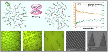
The photoresist is one of the key materials for the development of the modern semiconductor industry, and it not only affects the chip manufacturing process but also has an important impact on performance. Photoresists with low dielectric properties have a critical impact on the fabrication process and performance of various chips and devices. In this paper, a silicone encapsulated photoresist with low dielectric properties is reported, and it demonstrates excellent film-forming properties and lithography patterning effects, with a line width of 10 μm and a line spacing, a low dielectric constant (Dk = 2.75), a high thermal decomposition temperature (T5 = 503.5 °C), a low coefficient of thermal expansion (CTE = 33.61 ppm per °C), and excellent mechanical properties of thin films. This type of resin has a photo-crosslinked double bond structure and a thermally cross-linked benzocyclobutene structure, in which the silicone branched structure gives the photoresist excellent patterning properties and the thermally crosslinked structure gives the film excellent thermal, electrical, and mechanical properties. The resin is expected to replace traditional polyimide photoresists and has important applications in the semiconductor industry.

 求助内容:
求助内容: 应助结果提醒方式:


