Luca Panarella, Ben Kaczer, Quentin Smets, Stanislav Tyaginov, Pablo Saraza Canflanca, Andrea Vici, Devin Verreck, Tom Schram, Dennis Lin, Theresia Knobloch, Tibor Grasser, César Lockhart de la Rosa, Gouri S. Kar, Valeri Afanas’ev
{"title":"工业化生产的高尺度 MoS2 FET 中接触诱发变异的证据","authors":"Luca Panarella, Ben Kaczer, Quentin Smets, Stanislav Tyaginov, Pablo Saraza Canflanca, Andrea Vici, Devin Verreck, Tom Schram, Dennis Lin, Theresia Knobloch, Tibor Grasser, César Lockhart de la Rosa, Gouri S. Kar, Valeri Afanas’ev","doi":"10.1038/s41699-024-00482-9","DOIUrl":null,"url":null,"abstract":"Evidence of microscopic inhomogeneities of the side source/drain contacts in 300 mm wafer integrated MoS2 field-effect transistors is presented. In particular, the presence of a limited number of low Schottky barrier spots through which channel carriers are predominantly injected is demonstrated by the dramatic current changes induced by individual charge traps located near the source contact. Two distinct types of “contact-impacting traps” are identified. Type-1 trap is adjacent to the contact interface and exchanges carriers with the metal. Its impact is only observable when the adjacent contact is the reverse-biased FET source and limits the channel current. Type-2 trap is located in the AlOx gate oxide interlayer, near the source contact, and exchanges carriers with the channel. Its capture/emission time constants exhibit both a gate and drain bias dependence due to the high sensitivity of the contact regions to the applied lateral and vertical fields. Unlike typical channel-impacting oxide traps, both types of reported defects affect the Schottky barrier height and width rather than the threshold voltage and result in giant random telegraph noise (RTN). These observations indicate that the contact quality and geometry play a fundamental role in the ultimate scaling of 2D FETs.","PeriodicalId":19227,"journal":{"name":"npj 2D Materials and Applications","volume":" ","pages":"1-9"},"PeriodicalIF":9.1000,"publicationDate":"2024-07-14","publicationTypes":"Journal Article","fieldsOfStudy":null,"isOpenAccess":false,"openAccessPdf":"https://www.nature.com/articles/s41699-024-00482-9.pdf","citationCount":"0","resultStr":"{\"title\":\"Evidence of contact-induced variability in industrially-fabricated highly-scaled MoS2 FETs\",\"authors\":\"Luca Panarella, Ben Kaczer, Quentin Smets, Stanislav Tyaginov, Pablo Saraza Canflanca, Andrea Vici, Devin Verreck, Tom Schram, Dennis Lin, Theresia Knobloch, Tibor Grasser, César Lockhart de la Rosa, Gouri S. Kar, Valeri Afanas’ev\",\"doi\":\"10.1038/s41699-024-00482-9\",\"DOIUrl\":null,\"url\":null,\"abstract\":\"Evidence of microscopic inhomogeneities of the side source/drain contacts in 300 mm wafer integrated MoS2 field-effect transistors is presented. In particular, the presence of a limited number of low Schottky barrier spots through which channel carriers are predominantly injected is demonstrated by the dramatic current changes induced by individual charge traps located near the source contact. Two distinct types of “contact-impacting traps” are identified. Type-1 trap is adjacent to the contact interface and exchanges carriers with the metal. Its impact is only observable when the adjacent contact is the reverse-biased FET source and limits the channel current. Type-2 trap is located in the AlOx gate oxide interlayer, near the source contact, and exchanges carriers with the channel. Its capture/emission time constants exhibit both a gate and drain bias dependence due to the high sensitivity of the contact regions to the applied lateral and vertical fields. Unlike typical channel-impacting oxide traps, both types of reported defects affect the Schottky barrier height and width rather than the threshold voltage and result in giant random telegraph noise (RTN). These observations indicate that the contact quality and geometry play a fundamental role in the ultimate scaling of 2D FETs.\",\"PeriodicalId\":19227,\"journal\":{\"name\":\"npj 2D Materials and Applications\",\"volume\":\" \",\"pages\":\"1-9\"},\"PeriodicalIF\":9.1000,\"publicationDate\":\"2024-07-14\",\"publicationTypes\":\"Journal Article\",\"fieldsOfStudy\":null,\"isOpenAccess\":false,\"openAccessPdf\":\"https://www.nature.com/articles/s41699-024-00482-9.pdf\",\"citationCount\":\"0\",\"resultStr\":null,\"platform\":\"Semanticscholar\",\"paperid\":null,\"PeriodicalName\":\"npj 2D Materials and Applications\",\"FirstCategoryId\":\"88\",\"ListUrlMain\":\"https://www.nature.com/articles/s41699-024-00482-9\",\"RegionNum\":2,\"RegionCategory\":\"材料科学\",\"ArticlePicture\":[],\"TitleCN\":null,\"AbstractTextCN\":null,\"PMCID\":null,\"EPubDate\":\"\",\"PubModel\":\"\",\"JCR\":\"Q1\",\"JCRName\":\"MATERIALS SCIENCE, MULTIDISCIPLINARY\",\"Score\":null,\"Total\":0}","platform":"Semanticscholar","paperid":null,"PeriodicalName":"npj 2D Materials and Applications","FirstCategoryId":"88","ListUrlMain":"https://www.nature.com/articles/s41699-024-00482-9","RegionNum":2,"RegionCategory":"材料科学","ArticlePicture":[],"TitleCN":null,"AbstractTextCN":null,"PMCID":null,"EPubDate":"","PubModel":"","JCR":"Q1","JCRName":"MATERIALS SCIENCE, MULTIDISCIPLINARY","Score":null,"Total":0}
Evidence of contact-induced variability in industrially-fabricated highly-scaled MoS2 FETs
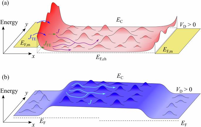
Evidence of microscopic inhomogeneities of the side source/drain contacts in 300 mm wafer integrated MoS2 field-effect transistors is presented. In particular, the presence of a limited number of low Schottky barrier spots through which channel carriers are predominantly injected is demonstrated by the dramatic current changes induced by individual charge traps located near the source contact. Two distinct types of “contact-impacting traps” are identified. Type-1 trap is adjacent to the contact interface and exchanges carriers with the metal. Its impact is only observable when the adjacent contact is the reverse-biased FET source and limits the channel current. Type-2 trap is located in the AlOx gate oxide interlayer, near the source contact, and exchanges carriers with the channel. Its capture/emission time constants exhibit both a gate and drain bias dependence due to the high sensitivity of the contact regions to the applied lateral and vertical fields. Unlike typical channel-impacting oxide traps, both types of reported defects affect the Schottky barrier height and width rather than the threshold voltage and result in giant random telegraph noise (RTN). These observations indicate that the contact quality and geometry play a fundamental role in the ultimate scaling of 2D FETs.
期刊介绍:
npj 2D Materials and Applications publishes papers on the fundamental behavior, synthesis, properties and applications of existing and emerging 2D materials. By selecting papers with the potential for impact, the journal aims to facilitate the transfer of the research of 2D materials into wide-ranging applications.