Satish Shetty, Andrian V. Kuchuk, Fernando Maia de Oliveira, Serhii Kryvyi, Chen Li, Paul Minor, Mohammad Zamani-Alavijeh, Nirosh M. Eldose, Subhashis Das, Dinesh Baral, Yuriy I. Mazur, H. Alan Mantooth, Gregory J. Salamo
{"title":"利用薄 InGaN 压缩应变梯度层提高 InN 薄膜质量","authors":"Satish Shetty, Andrian V. Kuchuk, Fernando Maia de Oliveira, Serhii Kryvyi, Chen Li, Paul Minor, Mohammad Zamani-Alavijeh, Nirosh M. Eldose, Subhashis Das, Dinesh Baral, Yuriy I. Mazur, H. Alan Mantooth, Gregory J. Salamo","doi":"10.1021/acs.cgd.4c00095","DOIUrl":null,"url":null,"abstract":"High-quality InN has significant opportunities for exciting and impactful electronic and photonic applications. These applications rely on growth techniques that produce high-quality InN thin films. To achieve the fabrication of InN semiconductor thin films with a low density of misfit and threading dislocations, we report on a growth technique that utilizes composition and strain gradients to limit the propagation of defects into InN grown on a GaN/sapphire substrate. The growth technique we have investigated utilizes a compressively strained gradient transition layer to limit the propagation of threading dislocations from the GaN buffer. Reflection high-energy electron diffraction, high-resolution X-ray diffraction, Raman spectroscopy, photoluminescence, and Hall measurements were employed to evaluate the effectiveness of the gradient transition layer to improve the quality of InN thin films. The outcome is that for InN films grown on partially graded In<sub><i>x</i></sub>Ga<sub>1–<i>x</i></sub>N (<i>x</i> → 0 to 29%), when compared with InN grown directly on a GaN substrate, we observed about a 40% decrease in edge dislocations, a 50% increase in photoluminescence, and a 20% increase in mobility. When compared to a sharp strain boundary, a linear strain gradient offers threading dislocations the opportunity to reduce the energy of the system more by leaving the system than by propagating into the strained region.","PeriodicalId":34,"journal":{"name":"Crystal Growth & Design","volume":"88 1","pages":""},"PeriodicalIF":3.4000,"publicationDate":"2024-07-09","publicationTypes":"Journal Article","fieldsOfStudy":null,"isOpenAccess":false,"openAccessPdf":"","citationCount":"0","resultStr":"{\"title\":\"Improved Quality of InN Thin Films Using a Thin InGaN Compressive Strain Gradient Layer\",\"authors\":\"Satish Shetty, Andrian V. Kuchuk, Fernando Maia de Oliveira, Serhii Kryvyi, Chen Li, Paul Minor, Mohammad Zamani-Alavijeh, Nirosh M. Eldose, Subhashis Das, Dinesh Baral, Yuriy I. Mazur, H. Alan Mantooth, Gregory J. Salamo\",\"doi\":\"10.1021/acs.cgd.4c00095\",\"DOIUrl\":null,\"url\":null,\"abstract\":\"High-quality InN has significant opportunities for exciting and impactful electronic and photonic applications. These applications rely on growth techniques that produce high-quality InN thin films. To achieve the fabrication of InN semiconductor thin films with a low density of misfit and threading dislocations, we report on a growth technique that utilizes composition and strain gradients to limit the propagation of defects into InN grown on a GaN/sapphire substrate. The growth technique we have investigated utilizes a compressively strained gradient transition layer to limit the propagation of threading dislocations from the GaN buffer. Reflection high-energy electron diffraction, high-resolution X-ray diffraction, Raman spectroscopy, photoluminescence, and Hall measurements were employed to evaluate the effectiveness of the gradient transition layer to improve the quality of InN thin films. The outcome is that for InN films grown on partially graded In<sub><i>x</i></sub>Ga<sub>1–<i>x</i></sub>N (<i>x</i> → 0 to 29%), when compared with InN grown directly on a GaN substrate, we observed about a 40% decrease in edge dislocations, a 50% increase in photoluminescence, and a 20% increase in mobility. When compared to a sharp strain boundary, a linear strain gradient offers threading dislocations the opportunity to reduce the energy of the system more by leaving the system than by propagating into the strained region.\",\"PeriodicalId\":34,\"journal\":{\"name\":\"Crystal Growth & Design\",\"volume\":\"88 1\",\"pages\":\"\"},\"PeriodicalIF\":3.4000,\"publicationDate\":\"2024-07-09\",\"publicationTypes\":\"Journal Article\",\"fieldsOfStudy\":null,\"isOpenAccess\":false,\"openAccessPdf\":\"\",\"citationCount\":\"0\",\"resultStr\":null,\"platform\":\"Semanticscholar\",\"paperid\":null,\"PeriodicalName\":\"Crystal Growth & Design\",\"FirstCategoryId\":\"92\",\"ListUrlMain\":\"https://doi.org/10.1021/acs.cgd.4c00095\",\"RegionNum\":2,\"RegionCategory\":\"化学\",\"ArticlePicture\":[],\"TitleCN\":null,\"AbstractTextCN\":null,\"PMCID\":null,\"EPubDate\":\"\",\"PubModel\":\"\",\"JCR\":\"Q2\",\"JCRName\":\"CHEMISTRY, MULTIDISCIPLINARY\",\"Score\":null,\"Total\":0}","platform":"Semanticscholar","paperid":null,"PeriodicalName":"Crystal Growth & Design","FirstCategoryId":"92","ListUrlMain":"https://doi.org/10.1021/acs.cgd.4c00095","RegionNum":2,"RegionCategory":"化学","ArticlePicture":[],"TitleCN":null,"AbstractTextCN":null,"PMCID":null,"EPubDate":"","PubModel":"","JCR":"Q2","JCRName":"CHEMISTRY, MULTIDISCIPLINARY","Score":null,"Total":0}
引用次数: 0
摘要
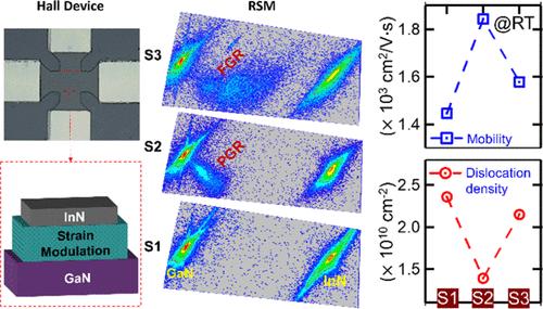
高质量的铟和氮化镓在电子和光子应用中有着令人兴奋和影响深远的重大机遇。这些应用依赖于能生产出高质量 InN 薄膜的生长技术。为了制造具有低错位和穿线位错密度的氮化铟半导体薄膜,我们报告了一种生长技术,它利用成分和应变梯度来限制生长在氮化镓/蓝宝石衬底上的氮化铟的缺陷传播。我们研究的生长技术利用压缩应变梯度过渡层来限制穿线位错从氮化镓缓冲区的传播。我们利用反射高能电子衍射、高分辨率 X 射线衍射、拉曼光谱、光致发光和霍尔测量来评估梯度过渡层在提高 InN 薄膜质量方面的有效性。结果表明,对于生长在部分梯度 InxGa1-xN (x → 0 至 29%)上的 InN 薄膜,与直接生长在 GaN 衬底上的 InN 相比,我们观察到边缘位错减少了约 40%,光致发光增加了 50%,迁移率增加了 20%。与尖锐的应变边界相比,线性应变梯度为穿线位错提供了机会,使其更多地通过离开系统而不是传播到应变区域来降低系统能量。
Improved Quality of InN Thin Films Using a Thin InGaN Compressive Strain Gradient Layer
High-quality InN has significant opportunities for exciting and impactful electronic and photonic applications. These applications rely on growth techniques that produce high-quality InN thin films. To achieve the fabrication of InN semiconductor thin films with a low density of misfit and threading dislocations, we report on a growth technique that utilizes composition and strain gradients to limit the propagation of defects into InN grown on a GaN/sapphire substrate. The growth technique we have investigated utilizes a compressively strained gradient transition layer to limit the propagation of threading dislocations from the GaN buffer. Reflection high-energy electron diffraction, high-resolution X-ray diffraction, Raman spectroscopy, photoluminescence, and Hall measurements were employed to evaluate the effectiveness of the gradient transition layer to improve the quality of InN thin films. The outcome is that for InN films grown on partially graded InxGa1–xN (x → 0 to 29%), when compared with InN grown directly on a GaN substrate, we observed about a 40% decrease in edge dislocations, a 50% increase in photoluminescence, and a 20% increase in mobility. When compared to a sharp strain boundary, a linear strain gradient offers threading dislocations the opportunity to reduce the energy of the system more by leaving the system than by propagating into the strained region.
期刊介绍:
The aim of Crystal Growth & Design is to stimulate crossfertilization of knowledge among scientists and engineers working in the fields of crystal growth, crystal engineering, and the industrial application of crystalline materials.
Crystal Growth & Design publishes theoretical and experimental studies of the physical, chemical, and biological phenomena and processes related to the design, growth, and application of crystalline materials. Synergistic approaches originating from different disciplines and technologies and integrating the fields of crystal growth, crystal engineering, intermolecular interactions, and industrial application are encouraged.