{"title":"研究在通过 PECVD 技术低温生长 nc-Ge 薄膜的过程中掺入 B,以减轻沉积后吸氧带来的不想要的传导特性","authors":"Sukalyan Shyam, Debajyoti Das","doi":"10.1016/j.solmat.2024.113034","DOIUrl":null,"url":null,"abstract":"<div><p>Post-deposition O absorption is a common issue in low-temperature grown nc-Ge films, that makes the material unstable and induces high <em>n</em>-type electrical conductivity ∼10<sup>−2</sup> S cm<sup>−1</sup>. An attempt has been made to mitigate the oxygen absorption issue through B doping of the nc-Ge thin film network at a low deposition temperature of ∼220 °C, employing a conventional capacitively coupled PECVD. At a B<sub>2</sub>H<sub>6</sub> flow rate of 3.0 sccm, the incorporation of a restricted quantity of B maintains a narrow band gap of ∼1.04 eV, significantly low conductivity of ∼6.76 ×10<sup>−7</sup> S cm<sup>−1</sup>, activation energy ∼398 meV, and photosensitivity of 6.0. Spectroscopic studies indicated that B doping facilitated reduced O-intake in the nc-Ge matrix, possibly via passivating the grain boundary defects and dangling bonds in the amorphous matrix and inducing the preferential absorption of O atoms in the Ge–O<sub>2</sub> configuration compared to its Ge–O<sub>x</sub> (x < 2) counterpart. The diminished O-induced carriers and the supplied acceptor levels by the B dopants compensate for the inherent <em>n</em>-type carrier concentration. However, at higher B<sub>2</sub>H<sub>6</sub> flow rates, significant B incorporation in the film matrix introduces numerous defects, degrading the crystallinity, despite increasing its <em>p</em>-type conductivity to 2.16 ×10<sup>−5</sup> S cm<sup>−1</sup> and maintaining a narrow band gap. Organized switching in the type of conductivity from the <em>n</em>-type to <em>p</em>-type ensues via gradually rising the B-dopants within the nc-Ge thin film network during its growth, which deserves attention for specific device applications.</p></div>","PeriodicalId":429,"journal":{"name":"Solar Energy Materials and Solar Cells","volume":null,"pages":null},"PeriodicalIF":6.3000,"publicationDate":"2024-07-08","publicationTypes":"Journal Article","fieldsOfStudy":null,"isOpenAccess":false,"openAccessPdf":"","citationCount":"0","resultStr":"{\"title\":\"Studies on B-doping during low-temperature growth of nc-Ge thin films via PECVD to mitigate unwanted conduction characteristics from the post-deposition oxygen absorption\",\"authors\":\"Sukalyan Shyam, Debajyoti Das\",\"doi\":\"10.1016/j.solmat.2024.113034\",\"DOIUrl\":null,\"url\":null,\"abstract\":\"<div><p>Post-deposition O absorption is a common issue in low-temperature grown nc-Ge films, that makes the material unstable and induces high <em>n</em>-type electrical conductivity ∼10<sup>−2</sup> S cm<sup>−1</sup>. An attempt has been made to mitigate the oxygen absorption issue through B doping of the nc-Ge thin film network at a low deposition temperature of ∼220 °C, employing a conventional capacitively coupled PECVD. At a B<sub>2</sub>H<sub>6</sub> flow rate of 3.0 sccm, the incorporation of a restricted quantity of B maintains a narrow band gap of ∼1.04 eV, significantly low conductivity of ∼6.76 ×10<sup>−7</sup> S cm<sup>−1</sup>, activation energy ∼398 meV, and photosensitivity of 6.0. Spectroscopic studies indicated that B doping facilitated reduced O-intake in the nc-Ge matrix, possibly via passivating the grain boundary defects and dangling bonds in the amorphous matrix and inducing the preferential absorption of O atoms in the Ge–O<sub>2</sub> configuration compared to its Ge–O<sub>x</sub> (x < 2) counterpart. The diminished O-induced carriers and the supplied acceptor levels by the B dopants compensate for the inherent <em>n</em>-type carrier concentration. However, at higher B<sub>2</sub>H<sub>6</sub> flow rates, significant B incorporation in the film matrix introduces numerous defects, degrading the crystallinity, despite increasing its <em>p</em>-type conductivity to 2.16 ×10<sup>−5</sup> S cm<sup>−1</sup> and maintaining a narrow band gap. Organized switching in the type of conductivity from the <em>n</em>-type to <em>p</em>-type ensues via gradually rising the B-dopants within the nc-Ge thin film network during its growth, which deserves attention for specific device applications.</p></div>\",\"PeriodicalId\":429,\"journal\":{\"name\":\"Solar Energy Materials and Solar Cells\",\"volume\":null,\"pages\":null},\"PeriodicalIF\":6.3000,\"publicationDate\":\"2024-07-08\",\"publicationTypes\":\"Journal Article\",\"fieldsOfStudy\":null,\"isOpenAccess\":false,\"openAccessPdf\":\"\",\"citationCount\":\"0\",\"resultStr\":null,\"platform\":\"Semanticscholar\",\"paperid\":null,\"PeriodicalName\":\"Solar Energy Materials and Solar Cells\",\"FirstCategoryId\":\"88\",\"ListUrlMain\":\"https://www.sciencedirect.com/science/article/pii/S0927024824003465\",\"RegionNum\":2,\"RegionCategory\":\"材料科学\",\"ArticlePicture\":[],\"TitleCN\":null,\"AbstractTextCN\":null,\"PMCID\":null,\"EPubDate\":\"\",\"PubModel\":\"\",\"JCR\":\"Q2\",\"JCRName\":\"ENERGY & FUELS\",\"Score\":null,\"Total\":0}","platform":"Semanticscholar","paperid":null,"PeriodicalName":"Solar Energy Materials and Solar Cells","FirstCategoryId":"88","ListUrlMain":"https://www.sciencedirect.com/science/article/pii/S0927024824003465","RegionNum":2,"RegionCategory":"材料科学","ArticlePicture":[],"TitleCN":null,"AbstractTextCN":null,"PMCID":null,"EPubDate":"","PubModel":"","JCR":"Q2","JCRName":"ENERGY & FUELS","Score":null,"Total":0}
引用次数: 0
摘要
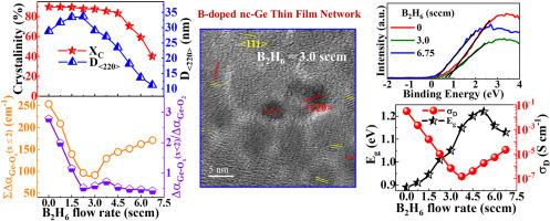
沉积后吸氧是低温生长的 nc-Ge 薄膜的一个常见问题,它会使材料变得不稳定,并导致 n 型电导率达到 10-2 S cm-1。我们尝试采用传统的电容耦合 PECVD 技术,在 220 ℃ 的低沉积温度下对 nc-Ge 薄膜网络进行 B 掺杂,以缓解氧气吸收问题。在 B2H6 流量为 3.0 sccm 的条件下,有限数量的 B 掺杂保持了 ∼1.04 eV 的窄带隙、∼6.76 ×10⁻⁷ S cm-1 的显著低电导率、∼398 meV 的活化能和 6.0 的光敏度。光谱研究表明,掺杂硼有助于减少 nc-Ge 基体中的 O 原子吸收,这可能是通过钝化晶界缺陷和无定形基体中的悬空键,以及诱导 Ge-O2 构型中的 O 原子优先吸收 Ge-Ox(x <2)构型中的 O 原子。O 诱导的载流子减少以及 B 掺杂剂提供的受体水平弥补了固有的 n 型载流子浓度。然而,在较高的 B2H6 流率下,尽管薄膜的 p 型电导率增加到 2.16 ×10⁻⁵ S cm-1,并保持了较窄的带隙,但在薄膜基质中大量掺入 B 会带来大量缺陷,降低结晶度。在 nc-Ge 薄膜网络的生长过程中,B-掺杂剂逐渐增加,从而实现了导电类型从 n 型到 p 型的有组织切换,这在特定器件应用中值得关注。
Studies on B-doping during low-temperature growth of nc-Ge thin films via PECVD to mitigate unwanted conduction characteristics from the post-deposition oxygen absorption
Post-deposition O absorption is a common issue in low-temperature grown nc-Ge films, that makes the material unstable and induces high n-type electrical conductivity ∼10−2 S cm−1. An attempt has been made to mitigate the oxygen absorption issue through B doping of the nc-Ge thin film network at a low deposition temperature of ∼220 °C, employing a conventional capacitively coupled PECVD. At a B2H6 flow rate of 3.0 sccm, the incorporation of a restricted quantity of B maintains a narrow band gap of ∼1.04 eV, significantly low conductivity of ∼6.76 ×10⁻⁷ S cm−1, activation energy ∼398 meV, and photosensitivity of 6.0. Spectroscopic studies indicated that B doping facilitated reduced O-intake in the nc-Ge matrix, possibly via passivating the grain boundary defects and dangling bonds in the amorphous matrix and inducing the preferential absorption of O atoms in the Ge–O2 configuration compared to its Ge–Ox (x < 2) counterpart. The diminished O-induced carriers and the supplied acceptor levels by the B dopants compensate for the inherent n-type carrier concentration. However, at higher B2H6 flow rates, significant B incorporation in the film matrix introduces numerous defects, degrading the crystallinity, despite increasing its p-type conductivity to 2.16 ×10⁻⁵ S cm−1 and maintaining a narrow band gap. Organized switching in the type of conductivity from the n-type to p-type ensues via gradually rising the B-dopants within the nc-Ge thin film network during its growth, which deserves attention for specific device applications.
期刊介绍:
Solar Energy Materials & Solar Cells is intended as a vehicle for the dissemination of research results on materials science and technology related to photovoltaic, photothermal and photoelectrochemical solar energy conversion. Materials science is taken in the broadest possible sense and encompasses physics, chemistry, optics, materials fabrication and analysis for all types of materials.
 求助内容:
求助内容: 应助结果提醒方式:


