了解二维材料的外延生长及其同质结构
IF 38.1
1区 材料科学
Q1 MATERIALS SCIENCE, MULTIDISCIPLINARY
引用次数: 0
摘要
二维(2D)范德华(vdW)材料的特殊物理特性已得到广泛研究,推动了材料合成的进步。外延生长作为一种重要的合成策略,能够生产出与先进集成电路兼容的大面积、高质量二维薄膜。典型的二维单晶体,如石墨烯、过渡金属二卤化物和六方氮化硼,已经在晶圆规模上实现了外延生长。需要进行系统总结,以便为新兴二维材料的外延提供战略指导。在此,我们主要从两个方向探讨二维 vdW 材料的外延方法:面内单晶单层的生长和面外同质结构的制造。我们首先讨论单个畴的成核控制和多个畴的取向控制,以实现大规模单晶单层。我们分析了采用各种外延生长技术的典型二维 vdW 材料的缺陷水平和晶体质量度量。然后,我们概述了生长均匀多层和扭曲同质结构的技术路线。我们进一步总结了当前的策略,以指导未来优化二维 vdW 材料的按需制造及其后续工业应用设备制造的工作。本文章由计算机程序翻译,如有差异,请以英文原文为准。
Understanding epitaxial growth of two-dimensional materials and their homostructures
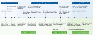
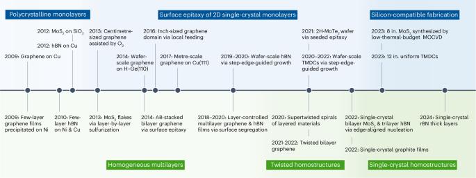
The exceptional physical properties of two-dimensional (2D) van der Waals (vdW) materials have been extensively researched, driving advances in material synthesis. Epitaxial growth, a prominent synthesis strategy, enables the production of large-area, high-quality 2D films compatible with advanced integrated circuits. Typical 2D single crystals, such as graphene, transition metal dichalcogenides and hexagonal boron nitride, have been epitaxially grown at a wafer scale. A systematic summary is required to offer strategic guidance for the epitaxy of emerging 2D materials. Here we focus on the epitaxy methodologies for 2D vdW materials in two directions: the growth of in-plane single-crystal monolayers and the fabrication of out-of-plane homostructures. We first discuss nucleation control of a single domain and orientation control over multiple domains to achieve large-scale single-crystal monolayers. We analyse the defect levels and measures of crystalline quality of typical 2D vdW materials with various epitaxial growth techniques. We then outline technical routes for the growth of homogeneous multilayers and twisted homostructures. We further summarize the current strategies to guide future efforts in optimizing on-demand fabrication of 2D vdW materials, as well as subsequent device manufacturing for their industrial applications. This Review examines conventional epitaxial growth of 2D van der Waals materials, focusing on in-plane single-crystal monolayer growth and out-of-plane homostructure fabrication. It covers nucleation and orientation control, quality control measures, and homogeneous multilayer and twisted homostructure growth techniques, providing systematic insights for on-demand fabrication of 2D van der Waals materials and their industrial device manufacturing.
求助全文
通过发布文献求助,成功后即可免费获取论文全文。
去求助
来源期刊
Nature nanotechnology
工程技术-材料科学:综合
CiteScore
59.70
自引率
0.80%
发文量
196
审稿时长
4-8 weeks
期刊介绍:
Nature Nanotechnology is a prestigious journal that publishes high-quality papers in various areas of nanoscience and nanotechnology. The journal focuses on the design, characterization, and production of structures, devices, and systems that manipulate and control materials at atomic, molecular, and macromolecular scales. It encompasses both bottom-up and top-down approaches, as well as their combinations.
Furthermore, Nature Nanotechnology fosters the exchange of ideas among researchers from diverse disciplines such as chemistry, physics, material science, biomedical research, engineering, and more. It promotes collaboration at the forefront of this multidisciplinary field. The journal covers a wide range of topics, from fundamental research in physics, chemistry, and biology, including computational work and simulations, to the development of innovative devices and technologies for various industrial sectors such as information technology, medicine, manufacturing, high-performance materials, energy, and environmental technologies. It includes coverage of organic, inorganic, and hybrid materials.
 求助内容:
求助内容: 应助结果提醒方式:


