三维集成金属氧化物晶体管

IF 33.7 1区 工程技术 Q1 ENGINEERING, ELECTRICAL & ELECTRONIC
Saravanan Yuvaraja, Hendrik Faber, Mritunjay Kumar, Na Xiao, Glen Isaac Maciel García, Xiao Tang, Thomas D. Anthopoulos, Xiaohang Li
{"title":"三维集成金属氧化物晶体管","authors":"Saravanan Yuvaraja, Hendrik Faber, Mritunjay Kumar, Na Xiao, Glen Isaac Maciel García, Xiao Tang, Thomas D. Anthopoulos, Xiaohang Li","doi":"10.1038/s41928-024-01205-0","DOIUrl":null,"url":null,"abstract":"The monolithic three-dimensional vertical integration of thin-film transistor (TFT) technologies could be used to create high-density, energy-efficient and low-cost integrated circuits. However, the development of scalable processes for integrating three-dimensional TFT devices is challenging. Here, we report the monolithic three-dimensional integration of indium oxide (In2O3) TFTs on a silicon/silicon dioxide (Si/SiO2) substrate at room temperature. We use an approach that is compatible with complementary metal–oxide–semiconductor (CMOS) processes to stack ten n-channel In2O3 TFTs. Different architectures—including bottom-, top- and dual-gate TFTs—can be fabricated at different layers in the stack. Our dual-gate devices exhibit enhanced electrical performance with a maximum field-effect mobility of 15 cm2 V−1 s−1, a subthreshold swing of 0.4 V dec−1 and a current on/off ratio of 108. By monolithically integrating dual-gate In2O3 TFTs at different locations in the stack, we created unipolar invertor circuits with a signal gain of around 50 and wide noise margins. The dual-gate devices also allow fine-tuning of the invertors to achieve symmetric voltage-transfer characteristics and optimal noise margins. A room-temperature approach to monolithic three-dimensional thin-film integration can be used to stack ten layers of n-channel indium oxide transistors on silicon/silicon dioxide substrates, while incorporating a range of architectures.","PeriodicalId":19064,"journal":{"name":"Nature Electronics","volume":null,"pages":null},"PeriodicalIF":33.7000,"publicationDate":"2024-07-08","publicationTypes":"Journal Article","fieldsOfStudy":null,"isOpenAccess":false,"openAccessPdf":"https://www.nature.com/articles/s41928-024-01205-0.pdf","citationCount":"0","resultStr":"{\"title\":\"Three-dimensional integrated metal-oxide transistors\",\"authors\":\"Saravanan Yuvaraja, Hendrik Faber, Mritunjay Kumar, Na Xiao, Glen Isaac Maciel García, Xiao Tang, Thomas D. Anthopoulos, Xiaohang Li\",\"doi\":\"10.1038/s41928-024-01205-0\",\"DOIUrl\":null,\"url\":null,\"abstract\":\"The monolithic three-dimensional vertical integration of thin-film transistor (TFT) technologies could be used to create high-density, energy-efficient and low-cost integrated circuits. However, the development of scalable processes for integrating three-dimensional TFT devices is challenging. Here, we report the monolithic three-dimensional integration of indium oxide (In2O3) TFTs on a silicon/silicon dioxide (Si/SiO2) substrate at room temperature. We use an approach that is compatible with complementary metal–oxide–semiconductor (CMOS) processes to stack ten n-channel In2O3 TFTs. Different architectures—including bottom-, top- and dual-gate TFTs—can be fabricated at different layers in the stack. Our dual-gate devices exhibit enhanced electrical performance with a maximum field-effect mobility of 15 cm2 V−1 s−1, a subthreshold swing of 0.4 V dec−1 and a current on/off ratio of 108. By monolithically integrating dual-gate In2O3 TFTs at different locations in the stack, we created unipolar invertor circuits with a signal gain of around 50 and wide noise margins. The dual-gate devices also allow fine-tuning of the invertors to achieve symmetric voltage-transfer characteristics and optimal noise margins. A room-temperature approach to monolithic three-dimensional thin-film integration can be used to stack ten layers of n-channel indium oxide transistors on silicon/silicon dioxide substrates, while incorporating a range of architectures.\",\"PeriodicalId\":19064,\"journal\":{\"name\":\"Nature Electronics\",\"volume\":null,\"pages\":null},\"PeriodicalIF\":33.7000,\"publicationDate\":\"2024-07-08\",\"publicationTypes\":\"Journal Article\",\"fieldsOfStudy\":null,\"isOpenAccess\":false,\"openAccessPdf\":\"https://www.nature.com/articles/s41928-024-01205-0.pdf\",\"citationCount\":\"0\",\"resultStr\":null,\"platform\":\"Semanticscholar\",\"paperid\":null,\"PeriodicalName\":\"Nature Electronics\",\"FirstCategoryId\":\"5\",\"ListUrlMain\":\"https://www.nature.com/articles/s41928-024-01205-0\",\"RegionNum\":1,\"RegionCategory\":\"工程技术\",\"ArticlePicture\":[],\"TitleCN\":null,\"AbstractTextCN\":null,\"PMCID\":null,\"EPubDate\":\"\",\"PubModel\":\"\",\"JCR\":\"Q1\",\"JCRName\":\"ENGINEERING, ELECTRICAL & ELECTRONIC\",\"Score\":null,\"Total\":0}","platform":"Semanticscholar","paperid":null,"PeriodicalName":"Nature Electronics","FirstCategoryId":"5","ListUrlMain":"https://www.nature.com/articles/s41928-024-01205-0","RegionNum":1,"RegionCategory":"工程技术","ArticlePicture":[],"TitleCN":null,"AbstractTextCN":null,"PMCID":null,"EPubDate":"","PubModel":"","JCR":"Q1","JCRName":"ENGINEERING, ELECTRICAL & ELECTRONIC","Score":null,"Total":0}
引用次数: 0

摘要

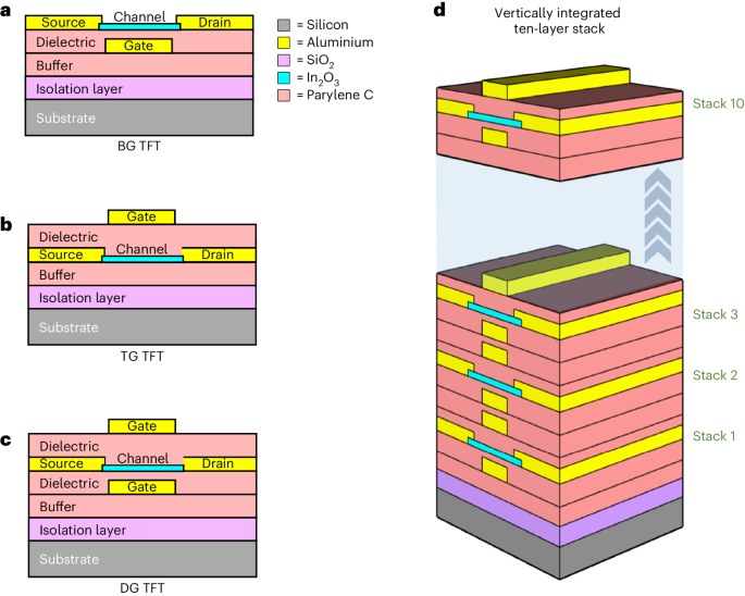
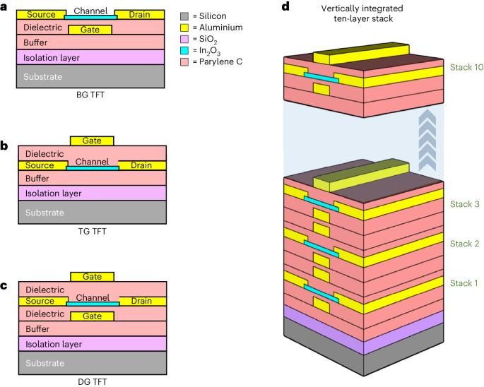
薄膜晶体管(TFT)技术的单片三维垂直集成可用于制造高密度、高能效和低成本的集成电路。然而,开发用于集成三维 TFT 器件的可扩展工艺具有挑战性。在此,我们报告了在室温下将氧化铟(In2O3)TFT 单片三维集成到硅/二氧化硅(Si/SiO2)衬底上的情况。我们采用一种与互补金属氧化物半导体(CMOS)工艺兼容的方法来堆叠十个 n 沟道 In2O3 TFT。在堆栈的不同层上可以制造出不同的结构,包括底部、顶部和双栅极 TFT。我们的双栅极器件具有更强的电气性能,最大场效应迁移率为 15 cm2 V-1 s-1,阈下摆幅为 0.4 V dec-1,电流开/关比为 108。通过在堆栈的不同位置单片集成双栅极 In2O3 TFT,我们创建了单极反相器电路,信号增益约为 50,噪声裕度大。双栅极器件还允许对反相器进行微调,以实现对称的电压传输特性和最佳的噪声裕度。
本文章由计算机程序翻译,如有差异,请以英文原文为准。

Three-dimensional integrated metal-oxide transistors

Three-dimensional integrated metal-oxide transistors

Three-dimensional integrated metal-oxide transistors
The monolithic three-dimensional vertical integration of thin-film transistor (TFT) technologies could be used to create high-density, energy-efficient and low-cost integrated circuits. However, the development of scalable processes for integrating three-dimensional TFT devices is challenging. Here, we report the monolithic three-dimensional integration of indium oxide (In2O3) TFTs on a silicon/silicon dioxide (Si/SiO2) substrate at room temperature. We use an approach that is compatible with complementary metal–oxide–semiconductor (CMOS) processes to stack ten n-channel In2O3 TFTs. Different architectures—including bottom-, top- and dual-gate TFTs—can be fabricated at different layers in the stack. Our dual-gate devices exhibit enhanced electrical performance with a maximum field-effect mobility of 15 cm2 V−1 s−1, a subthreshold swing of 0.4 V dec−1 and a current on/off ratio of 108. By monolithically integrating dual-gate In2O3 TFTs at different locations in the stack, we created unipolar invertor circuits with a signal gain of around 50 and wide noise margins. The dual-gate devices also allow fine-tuning of the invertors to achieve symmetric voltage-transfer characteristics and optimal noise margins. A room-temperature approach to monolithic three-dimensional thin-film integration can be used to stack ten layers of n-channel indium oxide transistors on silicon/silicon dioxide substrates, while incorporating a range of architectures.
求助全文
通过发布文献求助,成功后即可免费获取论文全文。 去求助
来源期刊
Nature Electronics
Nature Electronics Engineering-Electrical and Electronic Engineering
CiteScore
47.50
自引率
2.30%
发文量
159
期刊介绍: Nature Electronics is a comprehensive journal that publishes both fundamental and applied research in the field of electronics. It encompasses a wide range of topics, including the study of new phenomena and devices, the design and construction of electronic circuits, and the practical applications of electronics. In addition, the journal explores the commercial and industrial aspects of electronics research. The primary focus of Nature Electronics is on the development of technology and its potential impact on society. The journal incorporates the contributions of scientists, engineers, and industry professionals, offering a platform for their research findings. Moreover, Nature Electronics provides insightful commentary, thorough reviews, and analysis of the key issues that shape the field, as well as the technologies that are reshaping society. Like all journals within the prestigious Nature brand, Nature Electronics upholds the highest standards of quality. It maintains a dedicated team of professional editors and follows a fair and rigorous peer-review process. The journal also ensures impeccable copy-editing and production, enabling swift publication. Additionally, Nature Electronics prides itself on its editorial independence, ensuring unbiased and impartial reporting. In summary, Nature Electronics is a leading journal that publishes cutting-edge research in electronics. With its multidisciplinary approach and commitment to excellence, the journal serves as a valuable resource for scientists, engineers, and industry professionals seeking to stay at the forefront of advancements in the field.
×
引用
GB/T 7714-2015
复制
MLA
复制
APA
复制
导出至
BibTeX EndNote RefMan NoteFirst NoteExpress
×
提示
您的信息不完整,为了账户安全,请先补充。
现在去补充
×
提示
您因"违规操作"
具体请查看互助需知
我知道了
×
提示
确定
请完成安全验证×
copy
已复制链接
快去分享给好友吧!
我知道了
右上角分享
点击右上角分享
0
联系我们:info@booksci.cn Book学术提供免费学术资源搜索服务,方便国内外学者检索中英文文献。致力于提供最便捷和优质的服务体验。 Copyright © 2023 布克学术 All rights reserved.
京ICP备2023020795号-1
ghs 京公网安备 11010802042870号
Book学术文献互助
Book学术文献互助群
群 号:481959085
Book学术官方微信