Magdalena Grzeszczyk, Kristina Vaklinova, Kenji Watanabe, Takashi Taniguchi, Konstantin S. Novoselov, Maciej Koperski
{"title":"基于氢溴萘的垂直隧道结中纯谐振态的电致发光","authors":"Magdalena Grzeszczyk, Kristina Vaklinova, Kenji Watanabe, Takashi Taniguchi, Konstantin S. Novoselov, Maciej Koperski","doi":"10.1038/s41377-024-01491-5","DOIUrl":null,"url":null,"abstract":"<p>Defect centers in wide-band-gap crystals have garnered interest for their potential in applications among optoelectronic and sensor technologies. However, defects embedded in highly insulating crystals, like diamond, silicon carbide, or aluminum oxide, have been notoriously difficult to excite electrically due to their large internal resistance. To address this challenge, we realized a new paradigm of exciting defects in vertical tunneling junctions based on carbon centers in hexagonal boron nitride (hBN). The rational design of the devices via van der Waals technology enabled us to raise and control optical processes related to defect-to-band and intradefect electroluminescence. The fundamental understanding of the tunneling events was based on the transfer of the electronic wave function amplitude between resonant defect states in hBN to the metallic state in graphene, which leads to dramatic changes in the characteristics of electrons due to different band structures of constituent materials. In our devices, the decay of electrons via tunneling pathways competed with radiative recombination, resulting in an unprecedented degree of tuneability of carrier dynamics due to the significant sensitivity of the characteristic tunneling times on the thickness and structure of the barrier. This enabled us to achieve a high-efficiency electrical excitation of intradefect transitions, exceeding by several orders of magnitude the efficiency of optical excitation in the sub-band-gap regime. This work represents a significant advancement towards a universal and scalable platform for electrically driven devices utilizing defect centers in wide-band-gap crystals with properties modulated via activation of different tunneling mechanisms at a level of device engineering.</p>","PeriodicalId":18069,"journal":{"name":"Light-Science & Applications","volume":null,"pages":null},"PeriodicalIF":20.6000,"publicationDate":"2024-07-08","publicationTypes":"Journal Article","fieldsOfStudy":null,"isOpenAccess":false,"openAccessPdf":"","citationCount":"0","resultStr":"{\"title\":\"Electroluminescence from pure resonant states in hBN-based vertical tunneling junctions\",\"authors\":\"Magdalena Grzeszczyk, Kristina Vaklinova, Kenji Watanabe, Takashi Taniguchi, Konstantin S. Novoselov, Maciej Koperski\",\"doi\":\"10.1038/s41377-024-01491-5\",\"DOIUrl\":null,\"url\":null,\"abstract\":\"<p>Defect centers in wide-band-gap crystals have garnered interest for their potential in applications among optoelectronic and sensor technologies. However, defects embedded in highly insulating crystals, like diamond, silicon carbide, or aluminum oxide, have been notoriously difficult to excite electrically due to their large internal resistance. To address this challenge, we realized a new paradigm of exciting defects in vertical tunneling junctions based on carbon centers in hexagonal boron nitride (hBN). The rational design of the devices via van der Waals technology enabled us to raise and control optical processes related to defect-to-band and intradefect electroluminescence. The fundamental understanding of the tunneling events was based on the transfer of the electronic wave function amplitude between resonant defect states in hBN to the metallic state in graphene, which leads to dramatic changes in the characteristics of electrons due to different band structures of constituent materials. In our devices, the decay of electrons via tunneling pathways competed with radiative recombination, resulting in an unprecedented degree of tuneability of carrier dynamics due to the significant sensitivity of the characteristic tunneling times on the thickness and structure of the barrier. This enabled us to achieve a high-efficiency electrical excitation of intradefect transitions, exceeding by several orders of magnitude the efficiency of optical excitation in the sub-band-gap regime. This work represents a significant advancement towards a universal and scalable platform for electrically driven devices utilizing defect centers in wide-band-gap crystals with properties modulated via activation of different tunneling mechanisms at a level of device engineering.</p>\",\"PeriodicalId\":18069,\"journal\":{\"name\":\"Light-Science & Applications\",\"volume\":null,\"pages\":null},\"PeriodicalIF\":20.6000,\"publicationDate\":\"2024-07-08\",\"publicationTypes\":\"Journal Article\",\"fieldsOfStudy\":null,\"isOpenAccess\":false,\"openAccessPdf\":\"\",\"citationCount\":\"0\",\"resultStr\":null,\"platform\":\"Semanticscholar\",\"paperid\":null,\"PeriodicalName\":\"Light-Science & Applications\",\"FirstCategoryId\":\"1089\",\"ListUrlMain\":\"https://doi.org/10.1038/s41377-024-01491-5\",\"RegionNum\":0,\"RegionCategory\":null,\"ArticlePicture\":[],\"TitleCN\":null,\"AbstractTextCN\":null,\"PMCID\":null,\"EPubDate\":\"\",\"PubModel\":\"\",\"JCR\":\"Q1\",\"JCRName\":\"OPTICS\",\"Score\":null,\"Total\":0}","platform":"Semanticscholar","paperid":null,"PeriodicalName":"Light-Science & Applications","FirstCategoryId":"1089","ListUrlMain":"https://doi.org/10.1038/s41377-024-01491-5","RegionNum":0,"RegionCategory":null,"ArticlePicture":[],"TitleCN":null,"AbstractTextCN":null,"PMCID":null,"EPubDate":"","PubModel":"","JCR":"Q1","JCRName":"OPTICS","Score":null,"Total":0}
Electroluminescence from pure resonant states in hBN-based vertical tunneling junctions
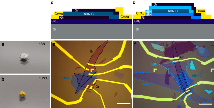
Defect centers in wide-band-gap crystals have garnered interest for their potential in applications among optoelectronic and sensor technologies. However, defects embedded in highly insulating crystals, like diamond, silicon carbide, or aluminum oxide, have been notoriously difficult to excite electrically due to their large internal resistance. To address this challenge, we realized a new paradigm of exciting defects in vertical tunneling junctions based on carbon centers in hexagonal boron nitride (hBN). The rational design of the devices via van der Waals technology enabled us to raise and control optical processes related to defect-to-band and intradefect electroluminescence. The fundamental understanding of the tunneling events was based on the transfer of the electronic wave function amplitude between resonant defect states in hBN to the metallic state in graphene, which leads to dramatic changes in the characteristics of electrons due to different band structures of constituent materials. In our devices, the decay of electrons via tunneling pathways competed with radiative recombination, resulting in an unprecedented degree of tuneability of carrier dynamics due to the significant sensitivity of the characteristic tunneling times on the thickness and structure of the barrier. This enabled us to achieve a high-efficiency electrical excitation of intradefect transitions, exceeding by several orders of magnitude the efficiency of optical excitation in the sub-band-gap regime. This work represents a significant advancement towards a universal and scalable platform for electrically driven devices utilizing defect centers in wide-band-gap crystals with properties modulated via activation of different tunneling mechanisms at a level of device engineering.
 求助内容:
求助内容: 应助结果提醒方式:


