Km. Sucheta Singh, Satyendra Kumar, Saurabh Chaturvedi, Kapil Dev Tyagi, Vaibhav Bhushan Tyagi
{"title":"器件和电路级掺砷化镓袖珍型双材料栅氧化物叠层 DG-TFET 性能评估","authors":"Km. Sucheta Singh, Satyendra Kumar, Saurabh Chaturvedi, Kapil Dev Tyagi, Vaibhav Bhushan Tyagi","doi":"10.1049/2024/9925894","DOIUrl":null,"url":null,"abstract":"<div>\n <p>This study explores the impact of integrating a gallium arsenide (GaAs) pocket at the source and drain in a dual-material gate-oxide-stack double-gate tunnel field-effect transistor (DMGOSDG-TFET). The performance of this DMGOSDG-TFET, employing work-function engineering and gate-oxide-stack techniques, is compared with a GaAs pocket-doped DMGOSDG-TFET. Using the Silvaco Technology Computer-Aided Design tool, the comparison covers DC characteristics, analog/RF behavior, and circuit-level assessments. The research introduces an optimized heterostructure pocket-doped DMGOSDG-TFET to enhance DC characteristics, analog/RF performance, and DC/transient analysis. This novel architecture effectively suppresses ambipolarity, making it more suitable for current conduction. The incorporation of work-function engineering and a gate-oxide-stack approach enhances the device’s current driving capability, while the use of a highly doped GaAs pocket at the source and drain virtually eliminates ambipolar current conduction. Simulation results indicate that the proposed heterostructure device exhibits a high ON-current and switching ratio. For analog/RF applications, the optimized heterostructure device outperforms conventional DMGOSDG-TFET, offering higher cutoff frequency, transconductance, and other analog/RF parameters. Circuit-level performance is assessed using HSPICE, with a focus on the implementation of a resistive-load inverter for both proposed and conventional device topologies through DC and transient evaluations.</p>\n </div>","PeriodicalId":50386,"journal":{"name":"Iet Circuits Devices & Systems","volume":"2024 1","pages":""},"PeriodicalIF":1.0000,"publicationDate":"2024-07-02","publicationTypes":"Journal Article","fieldsOfStudy":null,"isOpenAccess":false,"openAccessPdf":"https://onlinelibrary.wiley.com/doi/epdf/10.1049/2024/9925894","citationCount":"0","resultStr":"{\"title\":\"Performance Assessment of GaAs Pocket-Doped Dual-Material Gate-Oxide-Stack DG-TFET at Device and Circuit Level\",\"authors\":\"Km. Sucheta Singh, Satyendra Kumar, Saurabh Chaturvedi, Kapil Dev Tyagi, Vaibhav Bhushan Tyagi\",\"doi\":\"10.1049/2024/9925894\",\"DOIUrl\":null,\"url\":null,\"abstract\":\"<div>\\n <p>This study explores the impact of integrating a gallium arsenide (GaAs) pocket at the source and drain in a dual-material gate-oxide-stack double-gate tunnel field-effect transistor (DMGOSDG-TFET). The performance of this DMGOSDG-TFET, employing work-function engineering and gate-oxide-stack techniques, is compared with a GaAs pocket-doped DMGOSDG-TFET. Using the Silvaco Technology Computer-Aided Design tool, the comparison covers DC characteristics, analog/RF behavior, and circuit-level assessments. The research introduces an optimized heterostructure pocket-doped DMGOSDG-TFET to enhance DC characteristics, analog/RF performance, and DC/transient analysis. This novel architecture effectively suppresses ambipolarity, making it more suitable for current conduction. The incorporation of work-function engineering and a gate-oxide-stack approach enhances the device’s current driving capability, while the use of a highly doped GaAs pocket at the source and drain virtually eliminates ambipolar current conduction. Simulation results indicate that the proposed heterostructure device exhibits a high ON-current and switching ratio. For analog/RF applications, the optimized heterostructure device outperforms conventional DMGOSDG-TFET, offering higher cutoff frequency, transconductance, and other analog/RF parameters. Circuit-level performance is assessed using HSPICE, with a focus on the implementation of a resistive-load inverter for both proposed and conventional device topologies through DC and transient evaluations.</p>\\n </div>\",\"PeriodicalId\":50386,\"journal\":{\"name\":\"Iet Circuits Devices & Systems\",\"volume\":\"2024 1\",\"pages\":\"\"},\"PeriodicalIF\":1.0000,\"publicationDate\":\"2024-07-02\",\"publicationTypes\":\"Journal Article\",\"fieldsOfStudy\":null,\"isOpenAccess\":false,\"openAccessPdf\":\"https://onlinelibrary.wiley.com/doi/epdf/10.1049/2024/9925894\",\"citationCount\":\"0\",\"resultStr\":null,\"platform\":\"Semanticscholar\",\"paperid\":null,\"PeriodicalName\":\"Iet Circuits Devices & Systems\",\"FirstCategoryId\":\"5\",\"ListUrlMain\":\"https://onlinelibrary.wiley.com/doi/10.1049/2024/9925894\",\"RegionNum\":4,\"RegionCategory\":\"工程技术\",\"ArticlePicture\":[],\"TitleCN\":null,\"AbstractTextCN\":null,\"PMCID\":null,\"EPubDate\":\"\",\"PubModel\":\"\",\"JCR\":\"Q4\",\"JCRName\":\"ENGINEERING, ELECTRICAL & ELECTRONIC\",\"Score\":null,\"Total\":0}","platform":"Semanticscholar","paperid":null,"PeriodicalName":"Iet Circuits Devices & Systems","FirstCategoryId":"5","ListUrlMain":"https://onlinelibrary.wiley.com/doi/10.1049/2024/9925894","RegionNum":4,"RegionCategory":"工程技术","ArticlePicture":[],"TitleCN":null,"AbstractTextCN":null,"PMCID":null,"EPubDate":"","PubModel":"","JCR":"Q4","JCRName":"ENGINEERING, ELECTRICAL & ELECTRONIC","Score":null,"Total":0}
Performance Assessment of GaAs Pocket-Doped Dual-Material Gate-Oxide-Stack DG-TFET at Device and Circuit Level
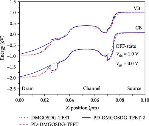
This study explores the impact of integrating a gallium arsenide (GaAs) pocket at the source and drain in a dual-material gate-oxide-stack double-gate tunnel field-effect transistor (DMGOSDG-TFET). The performance of this DMGOSDG-TFET, employing work-function engineering and gate-oxide-stack techniques, is compared with a GaAs pocket-doped DMGOSDG-TFET. Using the Silvaco Technology Computer-Aided Design tool, the comparison covers DC characteristics, analog/RF behavior, and circuit-level assessments. The research introduces an optimized heterostructure pocket-doped DMGOSDG-TFET to enhance DC characteristics, analog/RF performance, and DC/transient analysis. This novel architecture effectively suppresses ambipolarity, making it more suitable for current conduction. The incorporation of work-function engineering and a gate-oxide-stack approach enhances the device’s current driving capability, while the use of a highly doped GaAs pocket at the source and drain virtually eliminates ambipolar current conduction. Simulation results indicate that the proposed heterostructure device exhibits a high ON-current and switching ratio. For analog/RF applications, the optimized heterostructure device outperforms conventional DMGOSDG-TFET, offering higher cutoff frequency, transconductance, and other analog/RF parameters. Circuit-level performance is assessed using HSPICE, with a focus on the implementation of a resistive-load inverter for both proposed and conventional device topologies through DC and transient evaluations.
期刊介绍:
IET Circuits, Devices & Systems covers the following topics:
Circuit theory and design, circuit analysis and simulation, computer aided design
Filters (analogue and switched capacitor)
Circuit implementations, cells and architectures for integration including VLSI
Testability, fault tolerant design, minimisation of circuits and CAD for VLSI
Novel or improved electronic devices for both traditional and emerging technologies including nanoelectronics and MEMs
Device and process characterisation, device parameter extraction schemes
Mathematics of circuits and systems theory
Test and measurement techniques involving electronic circuits, circuits for industrial applications, sensors and transducers

 求助内容:
求助内容: 应助结果提醒方式:


