在 MIS 型二维异质结构中通过等离子体处理实现光学活性缺陷工程
IF 4.3
3区 材料科学
Q2 CHEMISTRY, MULTIDISCIPLINARY
引用次数: 0
摘要
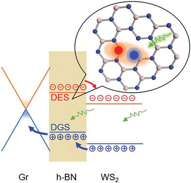
在二维异质结构的界面上,缺陷的存在及其操作对界面电荷转移行为起着至关重要的作用,并进一步影响器件的功能和性能。本研究探讨了 h-BN 层中故意引入的光活性缺陷对金属-绝缘体-半导体型异质结构器件的界面电荷转移和光响应性能的影响。利用电感耦合等离子体处理方法对缺陷的形成和浓度进行了定性控制,结果表明 h-BN 缺陷发射增强,石墨烯/h-BN 界面的石墨烯光学诱导掺杂效率更高。此外,在石墨烯和 WS2 之间使用 h-BN 层不仅能抑制暗态电荷载流子,而且由于缺陷水平的存在,还能促进光生电子-空穴对的分离和界面电荷转移,从而使异质结构光电探测器的光通/光断比和自驱动性能得到数量级的提高。这种控制绝缘层缺陷态的策略为优化二维界面的电荷转移过程提供了一种新方法,从而拓展了其在电子和光电器件领域的潜在应用。本文章由计算机程序翻译,如有差异,请以英文原文为准。
Optically Active Defect Engineering via Plasma Treatment in a MIS‐Type 2D Heterostructure
At the interface of 2D heterostructures, the presence of defects and their manipulation play a crucial role in the interfacial charge transfer behavior, further influencing the device functionality and performance. In this study, the impact of deliberately introduced photo‐active defects in the h‐BN layer on the interfacial charge transfer and photoresponse performance of a metal‐insulator‐semiconductor type heterostructure device is explored. The formation and concentration of defects are qualitatively controlled using an inductive coupled plasma treatment method, as evidenced by enhanced h‐BN defect emission and more efficient optically induced doping of graphene at the graphene/h‐BN interface. Besides, the use of the h‐BN layer between graphene and WS2 not only suppresses charge carriers in the dark state, but also promotes the separation of photo‐generated electron‐hole pairs and interfacial charge transfer due to the existence of defect levels, leading to orders of magnitude improvement in the light on/off ratio and self‐driving performance of the heterostructure photodetector. This strategy of controlling defect states in the insulating layer provides a new approach to optimize the charge transfer processes at the 2D interfaces, so as to expand its potential applications in the fields of electronic and optoelectronic devices.
求助全文
通过发布文献求助,成功后即可免费获取论文全文。
去求助
来源期刊
Advanced Materials Interfaces
CHEMISTRY, MULTIDISCIPLINARY-MATERIALS SCIENCE, MULTIDISCIPLINARY
CiteScore
8.40
自引率
5.60%
发文量
1174
审稿时长
1.3 months
期刊介绍:
Advanced Materials Interfaces publishes top-level research on interface technologies and effects. Considering any interface formed between solids, liquids, and gases, the journal ensures an interdisciplinary blend of physics, chemistry, materials science, and life sciences. Advanced Materials Interfaces was launched in 2014 and received an Impact Factor of 4.834 in 2018.
The scope of Advanced Materials Interfaces is dedicated to interfaces and surfaces that play an essential role in virtually all materials and devices. Physics, chemistry, materials science and life sciences blend to encourage new, cross-pollinating ideas, which will drive forward our understanding of the processes at the interface.
Advanced Materials Interfaces covers all topics in interface-related research:
Oil / water separation,
Applications of nanostructured materials,
2D materials and heterostructures,
Surfaces and interfaces in organic electronic devices,
Catalysis and membranes,
Self-assembly and nanopatterned surfaces,
Composite and coating materials,
Biointerfaces for technical and medical applications.
Advanced Materials Interfaces provides a forum for topics on surface and interface science with a wide choice of formats: Reviews, Full Papers, and Communications, as well as Progress Reports and Research News.
 求助内容:
求助内容: 应助结果提醒方式:


