Guobin Wang, Da Sheng, Yunfan Yang, Zesheng Zhang, Wenjun Wang and Hui Li*,
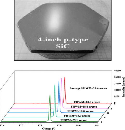
{"title":"具有高结晶质量的晶圆级 p 型碳化硅单晶体","authors":"Guobin Wang, Da Sheng, Yunfan Yang, Zesheng Zhang, Wenjun Wang and Hui Li*, ","doi":"10.1021/acs.cgd.4c00486","DOIUrl":null,"url":null,"abstract":"<p >Silicon carbide (SiC) single crystals are ideal platforms for fabrication of high-voltage, high-frequency, and high-temperature application devices, showing great potential applications in electric vehicles, photovoltaics, and rail transit. Among SiC-based devices, n-channel insulated gate bipolar transistors (IGBTs) show superior performances. However, their developments remain stagnant, predominantly ascribed to the lack of wafer-scale p-type SiC single crystals. Here, we report the breakthrough in the growth of 4-inch p-type 4H-SiC single crystals from high-temperature solutions with high crystalline quality and uniform doping. The average full width at half-maximum for the (0004) plane X-ray rocking curve is 19.4 arcsec and the resistivity deviation along the thickness direction is only 7.89%, outperforming those of the reported p-type SiC single crystals. The density of dislocation etching pits is 888.89 cm<sup>–2</sup>. The size of the dislocation etching pits is 1/10th of its counterpart grown by the physical vapor transport technique. The quality improvement is due to the removal of voids induced by gas bubbles, alongside the improvement of other growth parameters. The growth of wafer-scale p-type SiC opens a gate to the fabrication of n-channel SiC-based devices like n-IGBTs.</p>","PeriodicalId":34,"journal":{"name":"Crystal Growth & Design","volume":null,"pages":null},"PeriodicalIF":3.2000,"publicationDate":"2024-06-19","publicationTypes":"Journal Article","fieldsOfStudy":null,"isOpenAccess":false,"openAccessPdf":"","citationCount":"0","resultStr":"{\"title\":\"Wafer-Scale p-Type SiC Single Crystals with High Crystalline Quality\",\"authors\":\"Guobin Wang, Da Sheng, Yunfan Yang, Zesheng Zhang, Wenjun Wang and Hui Li*, \",\"doi\":\"10.1021/acs.cgd.4c00486\",\"DOIUrl\":null,\"url\":null,\"abstract\":\"<p >Silicon carbide (SiC) single crystals are ideal platforms for fabrication of high-voltage, high-frequency, and high-temperature application devices, showing great potential applications in electric vehicles, photovoltaics, and rail transit. Among SiC-based devices, n-channel insulated gate bipolar transistors (IGBTs) show superior performances. However, their developments remain stagnant, predominantly ascribed to the lack of wafer-scale p-type SiC single crystals. Here, we report the breakthrough in the growth of 4-inch p-type 4H-SiC single crystals from high-temperature solutions with high crystalline quality and uniform doping. The average full width at half-maximum for the (0004) plane X-ray rocking curve is 19.4 arcsec and the resistivity deviation along the thickness direction is only 7.89%, outperforming those of the reported p-type SiC single crystals. The density of dislocation etching pits is 888.89 cm<sup>–2</sup>. The size of the dislocation etching pits is 1/10th of its counterpart grown by the physical vapor transport technique. The quality improvement is due to the removal of voids induced by gas bubbles, alongside the improvement of other growth parameters. The growth of wafer-scale p-type SiC opens a gate to the fabrication of n-channel SiC-based devices like n-IGBTs.</p>\",\"PeriodicalId\":34,\"journal\":{\"name\":\"Crystal Growth & Design\",\"volume\":null,\"pages\":null},\"PeriodicalIF\":3.2000,\"publicationDate\":\"2024-06-19\",\"publicationTypes\":\"Journal Article\",\"fieldsOfStudy\":null,\"isOpenAccess\":false,\"openAccessPdf\":\"\",\"citationCount\":\"0\",\"resultStr\":null,\"platform\":\"Semanticscholar\",\"paperid\":null,\"PeriodicalName\":\"Crystal Growth & Design\",\"FirstCategoryId\":\"92\",\"ListUrlMain\":\"https://pubs.acs.org/doi/10.1021/acs.cgd.4c00486\",\"RegionNum\":2,\"RegionCategory\":\"化学\",\"ArticlePicture\":[],\"TitleCN\":null,\"AbstractTextCN\":null,\"PMCID\":null,\"EPubDate\":\"\",\"PubModel\":\"\",\"JCR\":\"Q2\",\"JCRName\":\"CHEMISTRY, MULTIDISCIPLINARY\",\"Score\":null,\"Total\":0}","platform":"Semanticscholar","paperid":null,"PeriodicalName":"Crystal Growth & Design","FirstCategoryId":"92","ListUrlMain":"https://pubs.acs.org/doi/10.1021/acs.cgd.4c00486","RegionNum":2,"RegionCategory":"化学","ArticlePicture":[],"TitleCN":null,"AbstractTextCN":null,"PMCID":null,"EPubDate":"","PubModel":"","JCR":"Q2","JCRName":"CHEMISTRY, MULTIDISCIPLINARY","Score":null,"Total":0}
引用次数: 0
摘要
碳化硅(SiC)单晶体是制造高压、高频和高温应用器件的理想平台,在电动汽车、光伏和轨道交通领域具有巨大的应用潜力。在碳化硅基器件中,n 沟道绝缘栅双极晶体管(IGBT)表现出卓越的性能。然而,其发展仍然停滞不前,主要原因是缺乏晶圆级 p 型碳化硅单晶。在此,我们报告了从高温溶液中生长出具有高结晶质量和均匀掺杂的 4 英寸 p 型 4H-SiC 单晶的突破性进展。(0004) 平面 X 射线摇摆曲线的平均半最大全宽为 19.4 弧秒,沿厚度方向的电阻率偏差仅为 7.89%,优于已报道的 p 型 SiC 单晶。位错蚀刻坑的密度为 888.89 cm-2。位错蚀刻坑的大小是通过物理气相传输技术生长的同类晶体的 1/10。质量提高的原因是除去了气泡引起的空隙,同时还改善了其他生长参数。晶圆级 p 型碳化硅的生长为制造 n-IGBT 等基于 n 沟道碳化硅的器件打开了大门。
Wafer-Scale p-Type SiC Single Crystals with High Crystalline Quality
Silicon carbide (SiC) single crystals are ideal platforms for fabrication of high-voltage, high-frequency, and high-temperature application devices, showing great potential applications in electric vehicles, photovoltaics, and rail transit. Among SiC-based devices, n-channel insulated gate bipolar transistors (IGBTs) show superior performances. However, their developments remain stagnant, predominantly ascribed to the lack of wafer-scale p-type SiC single crystals. Here, we report the breakthrough in the growth of 4-inch p-type 4H-SiC single crystals from high-temperature solutions with high crystalline quality and uniform doping. The average full width at half-maximum for the (0004) plane X-ray rocking curve is 19.4 arcsec and the resistivity deviation along the thickness direction is only 7.89%, outperforming those of the reported p-type SiC single crystals. The density of dislocation etching pits is 888.89 cm–2. The size of the dislocation etching pits is 1/10th of its counterpart grown by the physical vapor transport technique. The quality improvement is due to the removal of voids induced by gas bubbles, alongside the improvement of other growth parameters. The growth of wafer-scale p-type SiC opens a gate to the fabrication of n-channel SiC-based devices like n-IGBTs.
期刊介绍:
The aim of Crystal Growth & Design is to stimulate crossfertilization of knowledge among scientists and engineers working in the fields of crystal growth, crystal engineering, and the industrial application of crystalline materials.
Crystal Growth & Design publishes theoretical and experimental studies of the physical, chemical, and biological phenomena and processes related to the design, growth, and application of crystalline materials. Synergistic approaches originating from different disciplines and technologies and integrating the fields of crystal growth, crystal engineering, intermolecular interactions, and industrial application are encouraged.

 求助内容:
求助内容: 应助结果提醒方式:


