Maanwinder P. Singh, Qingxin Dong, Gen-Fu Chen, Alexander W. Holleitner and Christoph Kastl*,
{"title":"探测剥离 HfTe5 薄膜的空间均匀性。","authors":"Maanwinder P. Singh, Qingxin Dong, Gen-Fu Chen, Alexander W. Holleitner and Christoph Kastl*, ","doi":"10.1021/acsnano.4c02081","DOIUrl":null,"url":null,"abstract":"<p >In van der Waals materials, external strain is an effective tool to manipulate and control electronic responses by changing the electronic bands upon lattice deformation. In particular, the band gap of the layered transition metal pentatelluride HfTe<sub>5</sub> is sufficiently small to be inverted by subtle changes of the lattice parameters resulting in a strain-tunable topological phase transition. In that case, knowledge about the spatial homogeneity of electronic properties becomes crucial, especially for the microfabricated thin film circuits used in typical transport measurements. Here, we reveal the homogeneity of exfoliated HfTe<sub>5</sub> thin films by spatially resolved Raman microscopy. Comparing the Raman spectra under applied external strain to unstrained bulk references, we pinpoint local variations of Raman signatures to inhomogeneous strain profiles in the sample. Importantly, our results demonstrate that microfabricated contacts can act as sources of significant inhomogeneities. To mitigate the impact of unintentional strain and its corresponding modifications of the electronic structure, careful Raman microscopy constitutes a valuable tool for quantifying the homogeneity of HfTe<sub>5</sub> films and circuits fabricated thereof.</p>","PeriodicalId":21,"journal":{"name":"ACS Nano","volume":null,"pages":null},"PeriodicalIF":15.8000,"publicationDate":"2024-07-03","publicationTypes":"Journal Article","fieldsOfStudy":null,"isOpenAccess":false,"openAccessPdf":"https://pubs.acs.org/doi/epdf/10.1021/acsnano.4c02081","citationCount":"0","resultStr":"{\"title\":\"Probing the Spatial Homogeneity of Exfoliated HfTe5 Films\",\"authors\":\"Maanwinder P. Singh, Qingxin Dong, Gen-Fu Chen, Alexander W. Holleitner and Christoph Kastl*, \",\"doi\":\"10.1021/acsnano.4c02081\",\"DOIUrl\":null,\"url\":null,\"abstract\":\"<p >In van der Waals materials, external strain is an effective tool to manipulate and control electronic responses by changing the electronic bands upon lattice deformation. In particular, the band gap of the layered transition metal pentatelluride HfTe<sub>5</sub> is sufficiently small to be inverted by subtle changes of the lattice parameters resulting in a strain-tunable topological phase transition. In that case, knowledge about the spatial homogeneity of electronic properties becomes crucial, especially for the microfabricated thin film circuits used in typical transport measurements. Here, we reveal the homogeneity of exfoliated HfTe<sub>5</sub> thin films by spatially resolved Raman microscopy. Comparing the Raman spectra under applied external strain to unstrained bulk references, we pinpoint local variations of Raman signatures to inhomogeneous strain profiles in the sample. Importantly, our results demonstrate that microfabricated contacts can act as sources of significant inhomogeneities. To mitigate the impact of unintentional strain and its corresponding modifications of the electronic structure, careful Raman microscopy constitutes a valuable tool for quantifying the homogeneity of HfTe<sub>5</sub> films and circuits fabricated thereof.</p>\",\"PeriodicalId\":21,\"journal\":{\"name\":\"ACS Nano\",\"volume\":null,\"pages\":null},\"PeriodicalIF\":15.8000,\"publicationDate\":\"2024-07-03\",\"publicationTypes\":\"Journal Article\",\"fieldsOfStudy\":null,\"isOpenAccess\":false,\"openAccessPdf\":\"https://pubs.acs.org/doi/epdf/10.1021/acsnano.4c02081\",\"citationCount\":\"0\",\"resultStr\":null,\"platform\":\"Semanticscholar\",\"paperid\":null,\"PeriodicalName\":\"ACS Nano\",\"FirstCategoryId\":\"88\",\"ListUrlMain\":\"https://pubs.acs.org/doi/10.1021/acsnano.4c02081\",\"RegionNum\":1,\"RegionCategory\":\"材料科学\",\"ArticlePicture\":[],\"TitleCN\":null,\"AbstractTextCN\":null,\"PMCID\":null,\"EPubDate\":\"\",\"PubModel\":\"\",\"JCR\":\"Q1\",\"JCRName\":\"CHEMISTRY, MULTIDISCIPLINARY\",\"Score\":null,\"Total\":0}","platform":"Semanticscholar","paperid":null,"PeriodicalName":"ACS Nano","FirstCategoryId":"88","ListUrlMain":"https://pubs.acs.org/doi/10.1021/acsnano.4c02081","RegionNum":1,"RegionCategory":"材料科学","ArticlePicture":[],"TitleCN":null,"AbstractTextCN":null,"PMCID":null,"EPubDate":"","PubModel":"","JCR":"Q1","JCRName":"CHEMISTRY, MULTIDISCIPLINARY","Score":null,"Total":0}
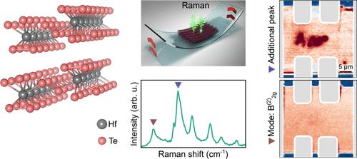
Probing the Spatial Homogeneity of Exfoliated HfTe5 Films
In van der Waals materials, external strain is an effective tool to manipulate and control electronic responses by changing the electronic bands upon lattice deformation. In particular, the band gap of the layered transition metal pentatelluride HfTe5 is sufficiently small to be inverted by subtle changes of the lattice parameters resulting in a strain-tunable topological phase transition. In that case, knowledge about the spatial homogeneity of electronic properties becomes crucial, especially for the microfabricated thin film circuits used in typical transport measurements. Here, we reveal the homogeneity of exfoliated HfTe5 thin films by spatially resolved Raman microscopy. Comparing the Raman spectra under applied external strain to unstrained bulk references, we pinpoint local variations of Raman signatures to inhomogeneous strain profiles in the sample. Importantly, our results demonstrate that microfabricated contacts can act as sources of significant inhomogeneities. To mitigate the impact of unintentional strain and its corresponding modifications of the electronic structure, careful Raman microscopy constitutes a valuable tool for quantifying the homogeneity of HfTe5 films and circuits fabricated thereof.
期刊介绍:
ACS Nano, published monthly, serves as an international forum for comprehensive articles on nanoscience and nanotechnology research at the intersections of chemistry, biology, materials science, physics, and engineering. The journal fosters communication among scientists in these communities, facilitating collaboration, new research opportunities, and advancements through discoveries. ACS Nano covers synthesis, assembly, characterization, theory, and simulation of nanostructures, nanobiotechnology, nanofabrication, methods and tools for nanoscience and nanotechnology, and self- and directed-assembly. Alongside original research articles, it offers thorough reviews, perspectives on cutting-edge research, and discussions envisioning the future of nanoscience and nanotechnology.


 求助内容:
求助内容: 应助结果提醒方式:


