Zhicheng Zhou, Juntong Zhu*, Lutao Li, Chen Wang, Changwen Zhang, Xinyu Du, Xiangyi Wang, Guoxiang Zhao, Ruonan Wang, Jiating Li, Zheng Lu, Yi Zong, Yinghui Sun, Mark H. Rümmeli* and Guifu Zou*,
{"title":"单分子膜辅助生长具有长寿命层间激子的卤化锑过氧化物/MoS2 范德华外延异质结。","authors":"Zhicheng Zhou, Juntong Zhu*, Lutao Li, Chen Wang, Changwen Zhang, Xinyu Du, Xiangyi Wang, Guoxiang Zhao, Ruonan Wang, Jiating Li, Zheng Lu, Yi Zong, Yinghui Sun, Mark H. Rümmeli* and Guifu Zou*, ","doi":"10.1021/acsnano.4c05293","DOIUrl":null,"url":null,"abstract":"<p >Epitaxial growth stands as a key method for integrating semiconductors into heterostructures, offering a potent avenue to explore the electronic and optoelectronic characteristics of cutting-edge materials, such as transition metal dichalcogenide (TMD) and perovskites. Nevertheless, the layer-by-layer growth atop TMD materials confronts a substantial energy barrier, impeding the adsorption and nucleation of perovskite atoms on the 2D surface. Here, we epitaxially grown an inorganic lead-free perovskite on TMD and formed van der Waals (vdW) heterojunctions. Our work employs a monomolecular membrane-assisted growth strategy that reduces the contact angle and simultaneously diminishing the energy barrier for Cs<sub>3</sub>Sb<sub>2</sub>Br<sub>9</sub> surface nucleation. By controlling the nucleation temperature, we achieved a reduction in the thickness of the Cs<sub>3</sub>Sb<sub>2</sub>Br<sub>9</sub> epitaxial layer from 30 to approximately 4 nm. In the realm of inorganic lead-free perovskite and TMD heterojunctions, we observed long-lived interlayer exciton of 9.9 ns, approximately 36 times longer than the intralayer exciton lifetime, which benefited from the excellent interlayer coupling brought by direct epitaxial growth. Our research introduces a monomolecular membrane-assisted growth strategy that expands the diversity of materials attainable through vdW epitaxial growth, potentially contributing to future applications in optoelectronics involving heterojunctions.</p>","PeriodicalId":21,"journal":{"name":"ACS Nano","volume":null,"pages":null},"PeriodicalIF":15.8000,"publicationDate":"2024-06-21","publicationTypes":"Journal Article","fieldsOfStudy":null,"isOpenAccess":false,"openAccessPdf":"","citationCount":"0","resultStr":"{\"title\":\"Monomolecular Membrane-Assisted Growth of Antimony Halide Perovskite/MoS2 Van der Waals Epitaxial Heterojunctions with Long-Lived Interlayer Exciton\",\"authors\":\"Zhicheng Zhou, Juntong Zhu*, Lutao Li, Chen Wang, Changwen Zhang, Xinyu Du, Xiangyi Wang, Guoxiang Zhao, Ruonan Wang, Jiating Li, Zheng Lu, Yi Zong, Yinghui Sun, Mark H. Rümmeli* and Guifu Zou*, \",\"doi\":\"10.1021/acsnano.4c05293\",\"DOIUrl\":null,\"url\":null,\"abstract\":\"<p >Epitaxial growth stands as a key method for integrating semiconductors into heterostructures, offering a potent avenue to explore the electronic and optoelectronic characteristics of cutting-edge materials, such as transition metal dichalcogenide (TMD) and perovskites. Nevertheless, the layer-by-layer growth atop TMD materials confronts a substantial energy barrier, impeding the adsorption and nucleation of perovskite atoms on the 2D surface. Here, we epitaxially grown an inorganic lead-free perovskite on TMD and formed van der Waals (vdW) heterojunctions. Our work employs a monomolecular membrane-assisted growth strategy that reduces the contact angle and simultaneously diminishing the energy barrier for Cs<sub>3</sub>Sb<sub>2</sub>Br<sub>9</sub> surface nucleation. By controlling the nucleation temperature, we achieved a reduction in the thickness of the Cs<sub>3</sub>Sb<sub>2</sub>Br<sub>9</sub> epitaxial layer from 30 to approximately 4 nm. In the realm of inorganic lead-free perovskite and TMD heterojunctions, we observed long-lived interlayer exciton of 9.9 ns, approximately 36 times longer than the intralayer exciton lifetime, which benefited from the excellent interlayer coupling brought by direct epitaxial growth. Our research introduces a monomolecular membrane-assisted growth strategy that expands the diversity of materials attainable through vdW epitaxial growth, potentially contributing to future applications in optoelectronics involving heterojunctions.</p>\",\"PeriodicalId\":21,\"journal\":{\"name\":\"ACS Nano\",\"volume\":null,\"pages\":null},\"PeriodicalIF\":15.8000,\"publicationDate\":\"2024-06-21\",\"publicationTypes\":\"Journal Article\",\"fieldsOfStudy\":null,\"isOpenAccess\":false,\"openAccessPdf\":\"\",\"citationCount\":\"0\",\"resultStr\":null,\"platform\":\"Semanticscholar\",\"paperid\":null,\"PeriodicalName\":\"ACS Nano\",\"FirstCategoryId\":\"88\",\"ListUrlMain\":\"https://pubs.acs.org/doi/10.1021/acsnano.4c05293\",\"RegionNum\":1,\"RegionCategory\":\"材料科学\",\"ArticlePicture\":[],\"TitleCN\":null,\"AbstractTextCN\":null,\"PMCID\":null,\"EPubDate\":\"\",\"PubModel\":\"\",\"JCR\":\"Q1\",\"JCRName\":\"CHEMISTRY, MULTIDISCIPLINARY\",\"Score\":null,\"Total\":0}","platform":"Semanticscholar","paperid":null,"PeriodicalName":"ACS Nano","FirstCategoryId":"88","ListUrlMain":"https://pubs.acs.org/doi/10.1021/acsnano.4c05293","RegionNum":1,"RegionCategory":"材料科学","ArticlePicture":[],"TitleCN":null,"AbstractTextCN":null,"PMCID":null,"EPubDate":"","PubModel":"","JCR":"Q1","JCRName":"CHEMISTRY, MULTIDISCIPLINARY","Score":null,"Total":0}
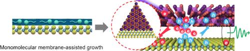
Monomolecular Membrane-Assisted Growth of Antimony Halide Perovskite/MoS2 Van der Waals Epitaxial Heterojunctions with Long-Lived Interlayer Exciton
Epitaxial growth stands as a key method for integrating semiconductors into heterostructures, offering a potent avenue to explore the electronic and optoelectronic characteristics of cutting-edge materials, such as transition metal dichalcogenide (TMD) and perovskites. Nevertheless, the layer-by-layer growth atop TMD materials confronts a substantial energy barrier, impeding the adsorption and nucleation of perovskite atoms on the 2D surface. Here, we epitaxially grown an inorganic lead-free perovskite on TMD and formed van der Waals (vdW) heterojunctions. Our work employs a monomolecular membrane-assisted growth strategy that reduces the contact angle and simultaneously diminishing the energy barrier for Cs3Sb2Br9 surface nucleation. By controlling the nucleation temperature, we achieved a reduction in the thickness of the Cs3Sb2Br9 epitaxial layer from 30 to approximately 4 nm. In the realm of inorganic lead-free perovskite and TMD heterojunctions, we observed long-lived interlayer exciton of 9.9 ns, approximately 36 times longer than the intralayer exciton lifetime, which benefited from the excellent interlayer coupling brought by direct epitaxial growth. Our research introduces a monomolecular membrane-assisted growth strategy that expands the diversity of materials attainable through vdW epitaxial growth, potentially contributing to future applications in optoelectronics involving heterojunctions.
期刊介绍:
ACS Nano, published monthly, serves as an international forum for comprehensive articles on nanoscience and nanotechnology research at the intersections of chemistry, biology, materials science, physics, and engineering. The journal fosters communication among scientists in these communities, facilitating collaboration, new research opportunities, and advancements through discoveries. ACS Nano covers synthesis, assembly, characterization, theory, and simulation of nanostructures, nanobiotechnology, nanofabrication, methods and tools for nanoscience and nanotechnology, and self- and directed-assembly. Alongside original research articles, it offers thorough reviews, perspectives on cutting-edge research, and discussions envisioning the future of nanoscience and nanotechnology.


 求助内容:
求助内容: 应助结果提醒方式:


