Abhishek Kumar, Jonas Müller, Sylvain Pelloquin, Aurélie Lecestre and Guilhem Larrieu*,
{"title":"基于三维垂直无结环栅晶体管的逻辑门与可靠的多级触点工程。","authors":"Abhishek Kumar, Jonas Müller, Sylvain Pelloquin, Aurélie Lecestre and Guilhem Larrieu*, ","doi":"10.1021/acs.nanolett.3c04180","DOIUrl":null,"url":null,"abstract":"<p >Vertical gate-all-around (V-GAA) represents the ultimate configuration in the forthcoming transistor industry, but it still encounters challenges in the semiconductor community. This paper introduces, for the first time, a dual-input logic gate circuit achieved using 3D vertical transistors with nanoscale sub-20-nm GAA, employing a novel technique for creating contacts and patterning metallic lines at the bottom level without the conventional lift-off process. This involves a two-step oxidation process: patterning the first field oxide to form bottom metal lines and then creating the gate oxide layer on nanowires (NWs), followed by selective removal from the top and bottom of the nanostructures. VGAA-NW transistors, fabricated using the lift-off-free approach, exhibit improved yield and reduced access resistance, leading to an enhanced drive current while maintaining good immunity against short-channel effects. Finally, elementary two-input logic gates within a single cell, using VNW transistors, demonstrate novel possibilities in advanced logic circuitry design and routing options in 3D.</p>","PeriodicalId":53,"journal":{"name":"Nano Letters","volume":null,"pages":null},"PeriodicalIF":9.6000,"publicationDate":"2024-06-17","publicationTypes":"Journal Article","fieldsOfStudy":null,"isOpenAccess":false,"openAccessPdf":"https://pubs.acs.org/doi/epdf/10.1021/acs.nanolett.3c04180","citationCount":"0","resultStr":"{\"title\":\"Logic Gates Based on 3D Vertical Junctionless Gate-All-Around Transistors with Reliable Multilevel Contact Engineering\",\"authors\":\"Abhishek Kumar, Jonas Müller, Sylvain Pelloquin, Aurélie Lecestre and Guilhem Larrieu*, \",\"doi\":\"10.1021/acs.nanolett.3c04180\",\"DOIUrl\":null,\"url\":null,\"abstract\":\"<p >Vertical gate-all-around (V-GAA) represents the ultimate configuration in the forthcoming transistor industry, but it still encounters challenges in the semiconductor community. This paper introduces, for the first time, a dual-input logic gate circuit achieved using 3D vertical transistors with nanoscale sub-20-nm GAA, employing a novel technique for creating contacts and patterning metallic lines at the bottom level without the conventional lift-off process. This involves a two-step oxidation process: patterning the first field oxide to form bottom metal lines and then creating the gate oxide layer on nanowires (NWs), followed by selective removal from the top and bottom of the nanostructures. VGAA-NW transistors, fabricated using the lift-off-free approach, exhibit improved yield and reduced access resistance, leading to an enhanced drive current while maintaining good immunity against short-channel effects. Finally, elementary two-input logic gates within a single cell, using VNW transistors, demonstrate novel possibilities in advanced logic circuitry design and routing options in 3D.</p>\",\"PeriodicalId\":53,\"journal\":{\"name\":\"Nano Letters\",\"volume\":null,\"pages\":null},\"PeriodicalIF\":9.6000,\"publicationDate\":\"2024-06-17\",\"publicationTypes\":\"Journal Article\",\"fieldsOfStudy\":null,\"isOpenAccess\":false,\"openAccessPdf\":\"https://pubs.acs.org/doi/epdf/10.1021/acs.nanolett.3c04180\",\"citationCount\":\"0\",\"resultStr\":null,\"platform\":\"Semanticscholar\",\"paperid\":null,\"PeriodicalName\":\"Nano Letters\",\"FirstCategoryId\":\"88\",\"ListUrlMain\":\"https://pubs.acs.org/doi/10.1021/acs.nanolett.3c04180\",\"RegionNum\":1,\"RegionCategory\":\"材料科学\",\"ArticlePicture\":[],\"TitleCN\":null,\"AbstractTextCN\":null,\"PMCID\":null,\"EPubDate\":\"\",\"PubModel\":\"\",\"JCR\":\"Q1\",\"JCRName\":\"CHEMISTRY, MULTIDISCIPLINARY\",\"Score\":null,\"Total\":0}","platform":"Semanticscholar","paperid":null,"PeriodicalName":"Nano Letters","FirstCategoryId":"88","ListUrlMain":"https://pubs.acs.org/doi/10.1021/acs.nanolett.3c04180","RegionNum":1,"RegionCategory":"材料科学","ArticlePicture":[],"TitleCN":null,"AbstractTextCN":null,"PMCID":null,"EPubDate":"","PubModel":"","JCR":"Q1","JCRName":"CHEMISTRY, MULTIDISCIPLINARY","Score":null,"Total":0}
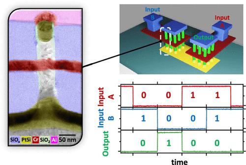
Logic Gates Based on 3D Vertical Junctionless Gate-All-Around Transistors with Reliable Multilevel Contact Engineering
Vertical gate-all-around (V-GAA) represents the ultimate configuration in the forthcoming transistor industry, but it still encounters challenges in the semiconductor community. This paper introduces, for the first time, a dual-input logic gate circuit achieved using 3D vertical transistors with nanoscale sub-20-nm GAA, employing a novel technique for creating contacts and patterning metallic lines at the bottom level without the conventional lift-off process. This involves a two-step oxidation process: patterning the first field oxide to form bottom metal lines and then creating the gate oxide layer on nanowires (NWs), followed by selective removal from the top and bottom of the nanostructures. VGAA-NW transistors, fabricated using the lift-off-free approach, exhibit improved yield and reduced access resistance, leading to an enhanced drive current while maintaining good immunity against short-channel effects. Finally, elementary two-input logic gates within a single cell, using VNW transistors, demonstrate novel possibilities in advanced logic circuitry design and routing options in 3D.
期刊介绍:
Nano Letters serves as a dynamic platform for promptly disseminating original results in fundamental, applied, and emerging research across all facets of nanoscience and nanotechnology. A pivotal criterion for inclusion within Nano Letters is the convergence of at least two different areas or disciplines, ensuring a rich interdisciplinary scope. The journal is dedicated to fostering exploration in diverse areas, including:
- Experimental and theoretical findings on physical, chemical, and biological phenomena at the nanoscale
- Synthesis, characterization, and processing of organic, inorganic, polymer, and hybrid nanomaterials through physical, chemical, and biological methodologies
- Modeling and simulation of synthetic, assembly, and interaction processes
- Realization of integrated nanostructures and nano-engineered devices exhibiting advanced performance
- Applications of nanoscale materials in living and environmental systems
Nano Letters is committed to advancing and showcasing groundbreaking research that intersects various domains, fostering innovation and collaboration in the ever-evolving field of nanoscience and nanotechnology.


 求助内容:
求助内容: 应助结果提醒方式:


