Joachim E. Sestoft*, Mikelis Marnauza, Dags Olsteins, Thomas Kanne, Rasmus D. Schlosser, I-Ju Chen, Kasper Grove-Rasmussen and Jesper Nygård*,
{"title":"Al/InAs 纳米线中的阴影与蚀刻超导体半导体结","authors":"Joachim E. Sestoft*, Mikelis Marnauza, Dags Olsteins, Thomas Kanne, Rasmus D. Schlosser, I-Ju Chen, Kasper Grove-Rasmussen and Jesper Nygård*, ","doi":"10.1021/acs.nanolett.4c02055","DOIUrl":null,"url":null,"abstract":"<p >Hybrid semiconductor–superconductor nanowires have emerged as a cornerstone in modern quantum devices. Integrating such nanowires into hybrid devices typically requires extensive postgrowth processing which may affect device performance unfavorably. Here, we present a technique for in situ shadowing superconductors on nanowires and compare the structural and electronic properties of Al junctions formed by shadowing versus etching. Based on transmission electron microscopy, we find that typical etching procedures lead to atomic-scale surface roughening. This surface perturbation may cause a reduction of the electron mobility as demonstrated in transport measurements. Further, we display advanced shadowing geometries aiding in the pursuit of bringing fabrication of hybrid devices in situ. Finally, we give examples of shadowed junctions exploited in various device geometries that exhibit high-quality quantum transport signatures.</p>","PeriodicalId":53,"journal":{"name":"Nano Letters","volume":"24 27","pages":"8394–8401"},"PeriodicalIF":9.1000,"publicationDate":"2024-06-12","publicationTypes":"Journal Article","fieldsOfStudy":null,"isOpenAccess":false,"openAccessPdf":"","citationCount":"0","resultStr":"{\"title\":\"Shadowed versus Etched Superconductor–Semiconductor Junctions in Al/InAs Nanowires\",\"authors\":\"Joachim E. Sestoft*, Mikelis Marnauza, Dags Olsteins, Thomas Kanne, Rasmus D. Schlosser, I-Ju Chen, Kasper Grove-Rasmussen and Jesper Nygård*, \",\"doi\":\"10.1021/acs.nanolett.4c02055\",\"DOIUrl\":null,\"url\":null,\"abstract\":\"<p >Hybrid semiconductor–superconductor nanowires have emerged as a cornerstone in modern quantum devices. Integrating such nanowires into hybrid devices typically requires extensive postgrowth processing which may affect device performance unfavorably. Here, we present a technique for in situ shadowing superconductors on nanowires and compare the structural and electronic properties of Al junctions formed by shadowing versus etching. Based on transmission electron microscopy, we find that typical etching procedures lead to atomic-scale surface roughening. This surface perturbation may cause a reduction of the electron mobility as demonstrated in transport measurements. Further, we display advanced shadowing geometries aiding in the pursuit of bringing fabrication of hybrid devices in situ. Finally, we give examples of shadowed junctions exploited in various device geometries that exhibit high-quality quantum transport signatures.</p>\",\"PeriodicalId\":53,\"journal\":{\"name\":\"Nano Letters\",\"volume\":\"24 27\",\"pages\":\"8394–8401\"},\"PeriodicalIF\":9.1000,\"publicationDate\":\"2024-06-12\",\"publicationTypes\":\"Journal Article\",\"fieldsOfStudy\":null,\"isOpenAccess\":false,\"openAccessPdf\":\"\",\"citationCount\":\"0\",\"resultStr\":null,\"platform\":\"Semanticscholar\",\"paperid\":null,\"PeriodicalName\":\"Nano Letters\",\"FirstCategoryId\":\"88\",\"ListUrlMain\":\"https://pubs.acs.org/doi/10.1021/acs.nanolett.4c02055\",\"RegionNum\":1,\"RegionCategory\":\"材料科学\",\"ArticlePicture\":[],\"TitleCN\":null,\"AbstractTextCN\":null,\"PMCID\":null,\"EPubDate\":\"\",\"PubModel\":\"\",\"JCR\":\"Q1\",\"JCRName\":\"CHEMISTRY, MULTIDISCIPLINARY\",\"Score\":null,\"Total\":0}","platform":"Semanticscholar","paperid":null,"PeriodicalName":"Nano Letters","FirstCategoryId":"88","ListUrlMain":"https://pubs.acs.org/doi/10.1021/acs.nanolett.4c02055","RegionNum":1,"RegionCategory":"材料科学","ArticlePicture":[],"TitleCN":null,"AbstractTextCN":null,"PMCID":null,"EPubDate":"","PubModel":"","JCR":"Q1","JCRName":"CHEMISTRY, MULTIDISCIPLINARY","Score":null,"Total":0}
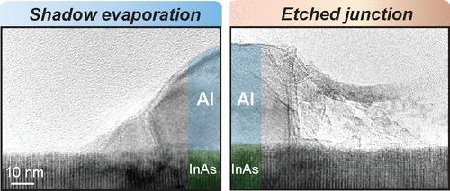
Shadowed versus Etched Superconductor–Semiconductor Junctions in Al/InAs Nanowires
Hybrid semiconductor–superconductor nanowires have emerged as a cornerstone in modern quantum devices. Integrating such nanowires into hybrid devices typically requires extensive postgrowth processing which may affect device performance unfavorably. Here, we present a technique for in situ shadowing superconductors on nanowires and compare the structural and electronic properties of Al junctions formed by shadowing versus etching. Based on transmission electron microscopy, we find that typical etching procedures lead to atomic-scale surface roughening. This surface perturbation may cause a reduction of the electron mobility as demonstrated in transport measurements. Further, we display advanced shadowing geometries aiding in the pursuit of bringing fabrication of hybrid devices in situ. Finally, we give examples of shadowed junctions exploited in various device geometries that exhibit high-quality quantum transport signatures.
期刊介绍:
Nano Letters serves as a dynamic platform for promptly disseminating original results in fundamental, applied, and emerging research across all facets of nanoscience and nanotechnology. A pivotal criterion for inclusion within Nano Letters is the convergence of at least two different areas or disciplines, ensuring a rich interdisciplinary scope. The journal is dedicated to fostering exploration in diverse areas, including:
- Experimental and theoretical findings on physical, chemical, and biological phenomena at the nanoscale
- Synthesis, characterization, and processing of organic, inorganic, polymer, and hybrid nanomaterials through physical, chemical, and biological methodologies
- Modeling and simulation of synthetic, assembly, and interaction processes
- Realization of integrated nanostructures and nano-engineered devices exhibiting advanced performance
- Applications of nanoscale materials in living and environmental systems
Nano Letters is committed to advancing and showcasing groundbreaking research that intersects various domains, fostering innovation and collaboration in the ever-evolving field of nanoscience and nanotechnology.


 求助内容:
求助内容: 应助结果提醒方式:


