{"title":"基于 TGV 的集成无源器件射频封装中低 k 材料的断裂情况","authors":"Luchao Wu , Lei Wang , Jun Wang","doi":"10.1016/j.mee.2024.112195","DOIUrl":null,"url":null,"abstract":"<div><p>The radio frequency (RF) chips and passive devices integrated on the through-glass-via (TGV) substrate meets the demands of miniaturization, high performance and low losses in the application. The RF chip and integrated passive devices (IPDs) are interconnected electrically by a redistribution layer (RDL) on the TGV substrate with the isolation low-k materials. The low-k materials, however, are susceptible to fracture during the thermal process in packaging due to their weak mechanical properties. In this study, the fractures of the low-k material were studied by experiments and the finite element analysis (FEA) for a RF package with integrated passive device based on TGV. The mechanical properties of the low-k material used in the FEA were tested by fabricating freestanding low-k films using microfabrication techniques. Then the fracture behaviors of the low-k material in the package and its impact factors under thermal loadings were examined. The impact factors, such as the initial defect location, direction and length, were investigated by evaluating the stress intensity factors (SIFs) at the defect tips. The results revealed that the most hazardous location in the low-k material is the region below the micro-joint of RF chip. The vertical defects along thickness in low-k film are more likely to propagate than horizontal ones. The SIF value increases linearly with the defect length both in heating and cooling conditions.</p></div>","PeriodicalId":18557,"journal":{"name":"Microelectronic Engineering","volume":"291 ","pages":"Article 112195"},"PeriodicalIF":2.6000,"publicationDate":"2024-06-08","publicationTypes":"Journal Article","fieldsOfStudy":null,"isOpenAccess":false,"openAccessPdf":"","citationCount":"0","resultStr":"{\"title\":\"Fractures of low-k materials in a RF package with integrated passive device based on TGV\",\"authors\":\"Luchao Wu , Lei Wang , Jun Wang\",\"doi\":\"10.1016/j.mee.2024.112195\",\"DOIUrl\":null,\"url\":null,\"abstract\":\"<div><p>The radio frequency (RF) chips and passive devices integrated on the through-glass-via (TGV) substrate meets the demands of miniaturization, high performance and low losses in the application. The RF chip and integrated passive devices (IPDs) are interconnected electrically by a redistribution layer (RDL) on the TGV substrate with the isolation low-k materials. The low-k materials, however, are susceptible to fracture during the thermal process in packaging due to their weak mechanical properties. In this study, the fractures of the low-k material were studied by experiments and the finite element analysis (FEA) for a RF package with integrated passive device based on TGV. The mechanical properties of the low-k material used in the FEA were tested by fabricating freestanding low-k films using microfabrication techniques. Then the fracture behaviors of the low-k material in the package and its impact factors under thermal loadings were examined. The impact factors, such as the initial defect location, direction and length, were investigated by evaluating the stress intensity factors (SIFs) at the defect tips. The results revealed that the most hazardous location in the low-k material is the region below the micro-joint of RF chip. The vertical defects along thickness in low-k film are more likely to propagate than horizontal ones. The SIF value increases linearly with the defect length both in heating and cooling conditions.</p></div>\",\"PeriodicalId\":18557,\"journal\":{\"name\":\"Microelectronic Engineering\",\"volume\":\"291 \",\"pages\":\"Article 112195\"},\"PeriodicalIF\":2.6000,\"publicationDate\":\"2024-06-08\",\"publicationTypes\":\"Journal Article\",\"fieldsOfStudy\":null,\"isOpenAccess\":false,\"openAccessPdf\":\"\",\"citationCount\":\"0\",\"resultStr\":null,\"platform\":\"Semanticscholar\",\"paperid\":null,\"PeriodicalName\":\"Microelectronic Engineering\",\"FirstCategoryId\":\"5\",\"ListUrlMain\":\"https://www.sciencedirect.com/science/article/pii/S0167931724000649\",\"RegionNum\":4,\"RegionCategory\":\"工程技术\",\"ArticlePicture\":[],\"TitleCN\":null,\"AbstractTextCN\":null,\"PMCID\":null,\"EPubDate\":\"\",\"PubModel\":\"\",\"JCR\":\"Q2\",\"JCRName\":\"ENGINEERING, ELECTRICAL & ELECTRONIC\",\"Score\":null,\"Total\":0}","platform":"Semanticscholar","paperid":null,"PeriodicalName":"Microelectronic Engineering","FirstCategoryId":"5","ListUrlMain":"https://www.sciencedirect.com/science/article/pii/S0167931724000649","RegionNum":4,"RegionCategory":"工程技术","ArticlePicture":[],"TitleCN":null,"AbstractTextCN":null,"PMCID":null,"EPubDate":"","PubModel":"","JCR":"Q2","JCRName":"ENGINEERING, ELECTRICAL & ELECTRONIC","Score":null,"Total":0}
引用次数: 0
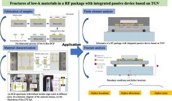
摘要
射频(RF)芯片和无源器件集成在穿透玻璃-导孔(TGV)基板上,可满足应用中对微型化、高性能和低损耗的要求。射频芯片和集成无源器件(IPD)通过 TGV 基底面上的再分布层(RDL)与隔离低 k 材料进行电气互连。然而,由于低 k 材料的机械性能较弱,在封装的热处理过程中容易发生断裂。本研究通过实验和有限元分析研究了基于 TGV 的集成无源器件射频封装中低 k 材料的断裂情况。有限元分析中使用的低 k 材料的机械性能是通过使用微加工技术制造独立的低 k 薄膜进行测试的。然后,研究了封装中低 k 材料在热负荷下的断裂行为及其影响因素。通过评估缺陷尖端的应力强度因子(SIF),研究了初始缺陷位置、方向和长度等影响因素。结果表明,低 K 材料中最危险的位置是射频芯片微连接处下方的区域。沿低 K 薄膜厚度方向的垂直缺陷比水平缺陷更容易传播。在加热和冷却条件下,SIF 值都随缺陷长度线性增加。
Fractures of low-k materials in a RF package with integrated passive device based on TGV
The radio frequency (RF) chips and passive devices integrated on the through-glass-via (TGV) substrate meets the demands of miniaturization, high performance and low losses in the application. The RF chip and integrated passive devices (IPDs) are interconnected electrically by a redistribution layer (RDL) on the TGV substrate with the isolation low-k materials. The low-k materials, however, are susceptible to fracture during the thermal process in packaging due to their weak mechanical properties. In this study, the fractures of the low-k material were studied by experiments and the finite element analysis (FEA) for a RF package with integrated passive device based on TGV. The mechanical properties of the low-k material used in the FEA were tested by fabricating freestanding low-k films using microfabrication techniques. Then the fracture behaviors of the low-k material in the package and its impact factors under thermal loadings were examined. The impact factors, such as the initial defect location, direction and length, were investigated by evaluating the stress intensity factors (SIFs) at the defect tips. The results revealed that the most hazardous location in the low-k material is the region below the micro-joint of RF chip. The vertical defects along thickness in low-k film are more likely to propagate than horizontal ones. The SIF value increases linearly with the defect length both in heating and cooling conditions.
期刊介绍:
Microelectronic Engineering is the premier nanoprocessing, and nanotechnology journal focusing on fabrication of electronic, photonic, bioelectronic, electromechanic and fluidic devices and systems, and their applications in the broad areas of electronics, photonics, energy, life sciences, and environment. It covers also the expanding interdisciplinary field of "more than Moore" and "beyond Moore" integrated nanoelectronics / photonics and micro-/nano-/bio-systems. Through its unique mixture of peer-reviewed articles, reviews, accelerated publications, short and Technical notes, and the latest research news on key developments, Microelectronic Engineering provides comprehensive coverage of this exciting, interdisciplinary and dynamic new field for researchers in academia and professionals in industry.

 求助内容:
求助内容: 应助结果提醒方式:


