Nehru Devabharathi, Sandeep Yadav, Inga Dönges, Vanessa Trouillet, Jörg J. Schneider
{"title":"用于低温加工薄膜晶体管器件的透明 p 型半导体 α-TeO2 氧化物(Adv.)","authors":"Nehru Devabharathi, Sandeep Yadav, Inga Dönges, Vanessa Trouillet, Jörg J. Schneider","doi":"10.1002/admi.202470041","DOIUrl":null,"url":null,"abstract":"<p><b><i>p</i>-Type Semiconductor</b></p><p><i>P</i>-type oxide semiconducting materials processable at or slightly above room temperature are still rare. Notably, a 5 nm <i>α</i>-TeO<sub>2</sub> thin film represents such an electronically active material and can be gas phase deposited into a thin film transistor device architecture. Nature sometimes creates it as para tellurite polymorph in beautiful single crystals as found in the Bambollita mine, Moctezuma, Sonora, Mexico. More details can be found in article number 2301082 by Jörg J. Schneider and co-workers. Cover image by Dr. S. Okeil. We thank Borja Sainz de Baranda Graf for the image of the crystal.\n\n <figure>\n <div><picture>\n <source></source></picture><p></p>\n </div>\n </figure></p>","PeriodicalId":115,"journal":{"name":"Advanced Materials Interfaces","volume":null,"pages":null},"PeriodicalIF":4.3000,"publicationDate":"2024-06-06","publicationTypes":"Journal Article","fieldsOfStudy":null,"isOpenAccess":false,"openAccessPdf":"https://onlinelibrary.wiley.com/doi/epdf/10.1002/admi.202470041","citationCount":"0","resultStr":"{\"title\":\"α-TeO2 Oxide as Transparent p-Type Semiconductor for Low Temperature Processed Thin Film Transistor Devices (Adv. Mater. Interfaces 16/2024)\",\"authors\":\"Nehru Devabharathi, Sandeep Yadav, Inga Dönges, Vanessa Trouillet, Jörg J. Schneider\",\"doi\":\"10.1002/admi.202470041\",\"DOIUrl\":null,\"url\":null,\"abstract\":\"<p><b><i>p</i>-Type Semiconductor</b></p><p><i>P</i>-type oxide semiconducting materials processable at or slightly above room temperature are still rare. Notably, a 5 nm <i>α</i>-TeO<sub>2</sub> thin film represents such an electronically active material and can be gas phase deposited into a thin film transistor device architecture. Nature sometimes creates it as para tellurite polymorph in beautiful single crystals as found in the Bambollita mine, Moctezuma, Sonora, Mexico. More details can be found in article number 2301082 by Jörg J. Schneider and co-workers. Cover image by Dr. S. Okeil. We thank Borja Sainz de Baranda Graf for the image of the crystal.\\n\\n <figure>\\n <div><picture>\\n <source></source></picture><p></p>\\n </div>\\n </figure></p>\",\"PeriodicalId\":115,\"journal\":{\"name\":\"Advanced Materials Interfaces\",\"volume\":null,\"pages\":null},\"PeriodicalIF\":4.3000,\"publicationDate\":\"2024-06-06\",\"publicationTypes\":\"Journal Article\",\"fieldsOfStudy\":null,\"isOpenAccess\":false,\"openAccessPdf\":\"https://onlinelibrary.wiley.com/doi/epdf/10.1002/admi.202470041\",\"citationCount\":\"0\",\"resultStr\":null,\"platform\":\"Semanticscholar\",\"paperid\":null,\"PeriodicalName\":\"Advanced Materials Interfaces\",\"FirstCategoryId\":\"88\",\"ListUrlMain\":\"https://onlinelibrary.wiley.com/doi/10.1002/admi.202470041\",\"RegionNum\":3,\"RegionCategory\":\"材料科学\",\"ArticlePicture\":[],\"TitleCN\":null,\"AbstractTextCN\":null,\"PMCID\":null,\"EPubDate\":\"\",\"PubModel\":\"\",\"JCR\":\"Q2\",\"JCRName\":\"CHEMISTRY, MULTIDISCIPLINARY\",\"Score\":null,\"Total\":0}","platform":"Semanticscholar","paperid":null,"PeriodicalName":"Advanced Materials Interfaces","FirstCategoryId":"88","ListUrlMain":"https://onlinelibrary.wiley.com/doi/10.1002/admi.202470041","RegionNum":3,"RegionCategory":"材料科学","ArticlePicture":[],"TitleCN":null,"AbstractTextCN":null,"PMCID":null,"EPubDate":"","PubModel":"","JCR":"Q2","JCRName":"CHEMISTRY, MULTIDISCIPLINARY","Score":null,"Total":0}
引用次数: 0
摘要
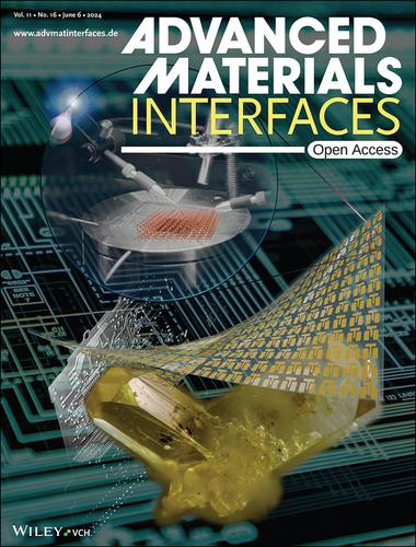
对型半导体可在室温或略高于室温条件下加工的对型氧化物半导体材料仍然十分罕见。值得注意的是,5 nm α-TeO2 薄膜就是这样一种电子活性材料,可以气相沉积到薄膜晶体管设备结构中。大自然有时会以美丽单晶体的对位碲多晶体形式创造这种材料,如在墨西哥索诺拉州莫克特祖马的班博利塔矿区发现的碲多晶体。更多详情,请参阅 Jörg J. Schneider 及其合作者撰写的第 2301082 号文章。封面图片由 S. Okeil 博士提供。感谢 Borja Sainz de Baranda Graf 提供晶体图片。
α-TeO2 Oxide as Transparent p-Type Semiconductor for Low Temperature Processed Thin Film Transistor Devices (Adv. Mater. Interfaces 16/2024)
p-Type Semiconductor
P-type oxide semiconducting materials processable at or slightly above room temperature are still rare. Notably, a 5 nm α-TeO2 thin film represents such an electronically active material and can be gas phase deposited into a thin film transistor device architecture. Nature sometimes creates it as para tellurite polymorph in beautiful single crystals as found in the Bambollita mine, Moctezuma, Sonora, Mexico. More details can be found in article number 2301082 by Jörg J. Schneider and co-workers. Cover image by Dr. S. Okeil. We thank Borja Sainz de Baranda Graf for the image of the crystal.
期刊介绍:
Advanced Materials Interfaces publishes top-level research on interface technologies and effects. Considering any interface formed between solids, liquids, and gases, the journal ensures an interdisciplinary blend of physics, chemistry, materials science, and life sciences. Advanced Materials Interfaces was launched in 2014 and received an Impact Factor of 4.834 in 2018.
The scope of Advanced Materials Interfaces is dedicated to interfaces and surfaces that play an essential role in virtually all materials and devices. Physics, chemistry, materials science and life sciences blend to encourage new, cross-pollinating ideas, which will drive forward our understanding of the processes at the interface.
Advanced Materials Interfaces covers all topics in interface-related research:
Oil / water separation,
Applications of nanostructured materials,
2D materials and heterostructures,
Surfaces and interfaces in organic electronic devices,
Catalysis and membranes,
Self-assembly and nanopatterned surfaces,
Composite and coating materials,
Biointerfaces for technical and medical applications.
Advanced Materials Interfaces provides a forum for topics on surface and interface science with a wide choice of formats: Reviews, Full Papers, and Communications, as well as Progress Reports and Research News.