{"title":"同极性化学键诱导层状半导体的平面内各向异性","authors":"Jieling Tan, Jiang-Jing Wang, Hang-Ming Zhang, Han-Yi Zhang, Heming Li, Yu Wang, Yuxing Zhou, Volker L. Deringer, Wei Zhang","doi":"10.1002/smsc.202400226","DOIUrl":null,"url":null,"abstract":"Main-group layered binary semiconductors, in particular, the III–VI alloys in the binary Ga–Te system are attracting increasing interest for a range of practical applications. The III–VI semiconductor, monoclinic gallium monotelluride (m-GaTe), has been recently used in high-sensitivity photodetectors/phototransistors and electronic memory applications due to its anisotropic properties yielding superior optical and electrical performance. Despite these applications, the origin of such anisotropy, namely the complex structural and bonding environments in GaTe nanostructures remain to be fully understood. In the present work, a comprehensive atomic-scale characterization of m-GaTe is reported by element-resolved atomic-scale microscopy experiments, enabling a direct measure of the in-plane anisotropy at the sub-Angstrom level. It is shown that these experimental images compare well with the results of first-principles modeling. Quantum-chemical bonding analyses provide a detailed picture of the atomic neighbor interactions within the layers, revealing that vertical Ga<span></span>Ga homopolar bonds get stronger when they are distorted and rotated, inducing the strong in-plane anisotropy. Beyond GaTe, using a systematic screening over the Materials Project database, the four additional low-symmetric layered crystals with similar distorted tetrahedral patterns are identified, indicating that the homopolar-bond-induced anisotropy is a more generic feature in these layered van der Waals (vdW) materials.","PeriodicalId":29791,"journal":{"name":"Small Science","volume":"43 1","pages":""},"PeriodicalIF":11.1000,"publicationDate":"2024-06-03","publicationTypes":"Journal Article","fieldsOfStudy":null,"isOpenAccess":false,"openAccessPdf":"","citationCount":"0","resultStr":"{\"title\":\"Homopolar Chemical Bonds Induce In-Plane Anisotropy in Layered Semiconductors\",\"authors\":\"Jieling Tan, Jiang-Jing Wang, Hang-Ming Zhang, Han-Yi Zhang, Heming Li, Yu Wang, Yuxing Zhou, Volker L. Deringer, Wei Zhang\",\"doi\":\"10.1002/smsc.202400226\",\"DOIUrl\":null,\"url\":null,\"abstract\":\"Main-group layered binary semiconductors, in particular, the III–VI alloys in the binary Ga–Te system are attracting increasing interest for a range of practical applications. The III–VI semiconductor, monoclinic gallium monotelluride (m-GaTe), has been recently used in high-sensitivity photodetectors/phototransistors and electronic memory applications due to its anisotropic properties yielding superior optical and electrical performance. Despite these applications, the origin of such anisotropy, namely the complex structural and bonding environments in GaTe nanostructures remain to be fully understood. In the present work, a comprehensive atomic-scale characterization of m-GaTe is reported by element-resolved atomic-scale microscopy experiments, enabling a direct measure of the in-plane anisotropy at the sub-Angstrom level. It is shown that these experimental images compare well with the results of first-principles modeling. Quantum-chemical bonding analyses provide a detailed picture of the atomic neighbor interactions within the layers, revealing that vertical Ga<span></span>Ga homopolar bonds get stronger when they are distorted and rotated, inducing the strong in-plane anisotropy. Beyond GaTe, using a systematic screening over the Materials Project database, the four additional low-symmetric layered crystals with similar distorted tetrahedral patterns are identified, indicating that the homopolar-bond-induced anisotropy is a more generic feature in these layered van der Waals (vdW) materials.\",\"PeriodicalId\":29791,\"journal\":{\"name\":\"Small Science\",\"volume\":\"43 1\",\"pages\":\"\"},\"PeriodicalIF\":11.1000,\"publicationDate\":\"2024-06-03\",\"publicationTypes\":\"Journal Article\",\"fieldsOfStudy\":null,\"isOpenAccess\":false,\"openAccessPdf\":\"\",\"citationCount\":\"0\",\"resultStr\":null,\"platform\":\"Semanticscholar\",\"paperid\":null,\"PeriodicalName\":\"Small Science\",\"FirstCategoryId\":\"1085\",\"ListUrlMain\":\"https://doi.org/10.1002/smsc.202400226\",\"RegionNum\":0,\"RegionCategory\":null,\"ArticlePicture\":[],\"TitleCN\":null,\"AbstractTextCN\":null,\"PMCID\":null,\"EPubDate\":\"\",\"PubModel\":\"\",\"JCR\":\"Q1\",\"JCRName\":\"MATERIALS SCIENCE, MULTIDISCIPLINARY\",\"Score\":null,\"Total\":0}","platform":"Semanticscholar","paperid":null,"PeriodicalName":"Small Science","FirstCategoryId":"1085","ListUrlMain":"https://doi.org/10.1002/smsc.202400226","RegionNum":0,"RegionCategory":null,"ArticlePicture":[],"TitleCN":null,"AbstractTextCN":null,"PMCID":null,"EPubDate":"","PubModel":"","JCR":"Q1","JCRName":"MATERIALS SCIENCE, MULTIDISCIPLINARY","Score":null,"Total":0}
Homopolar Chemical Bonds Induce In-Plane Anisotropy in Layered Semiconductors
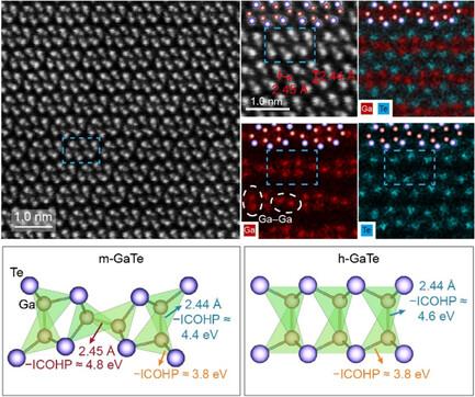
Main-group layered binary semiconductors, in particular, the III–VI alloys in the binary Ga–Te system are attracting increasing interest for a range of practical applications. The III–VI semiconductor, monoclinic gallium monotelluride (m-GaTe), has been recently used in high-sensitivity photodetectors/phototransistors and electronic memory applications due to its anisotropic properties yielding superior optical and electrical performance. Despite these applications, the origin of such anisotropy, namely the complex structural and bonding environments in GaTe nanostructures remain to be fully understood. In the present work, a comprehensive atomic-scale characterization of m-GaTe is reported by element-resolved atomic-scale microscopy experiments, enabling a direct measure of the in-plane anisotropy at the sub-Angstrom level. It is shown that these experimental images compare well with the results of first-principles modeling. Quantum-chemical bonding analyses provide a detailed picture of the atomic neighbor interactions within the layers, revealing that vertical GaGa homopolar bonds get stronger when they are distorted and rotated, inducing the strong in-plane anisotropy. Beyond GaTe, using a systematic screening over the Materials Project database, the four additional low-symmetric layered crystals with similar distorted tetrahedral patterns are identified, indicating that the homopolar-bond-induced anisotropy is a more generic feature in these layered van der Waals (vdW) materials.
期刊介绍:
Small Science is a premium multidisciplinary open access journal dedicated to publishing impactful research from all areas of nanoscience and nanotechnology. It features interdisciplinary original research and focused review articles on relevant topics. The journal covers design, characterization, mechanism, technology, and application of micro-/nanoscale structures and systems in various fields including physics, chemistry, materials science, engineering, environmental science, life science, biology, and medicine. It welcomes innovative interdisciplinary research and its readership includes professionals from academia and industry in fields such as chemistry, physics, materials science, biology, engineering, and environmental and analytical science. Small Science is indexed and abstracted in CAS, DOAJ, Clarivate Analytics, ProQuest Central, Publicly Available Content Database, Science Database, SCOPUS, and Web of Science.