Yoganash Putthisigamany, Kazi Sajedur Rahman, Megat Mohd Izhar Sapeli, Norasikin Ahmad Ludin, Mohd AdibIbrahim and Puvaneswaran Chelvanathan*,
{"title":"揭示直流刻蚀钼背接触功函数在减轻钾长石基薄膜太阳能电池中 MoS2/MoSe2 介面层的有害影响方面的微妙作用","authors":"Yoganash Putthisigamany, Kazi Sajedur Rahman, Megat Mohd Izhar Sapeli, Norasikin Ahmad Ludin, Mohd AdibIbrahim and Puvaneswaran Chelvanathan*, ","doi":"10.1021/acs.energyfuels.4c00512","DOIUrl":null,"url":null,"abstract":"<p >Due to thermal robustness and chemical stability at high working temperatures during photo-absorber layer deposition, molybdenum (Mo) is favored as the back electrode material in chalcogenide-based thin film photovoltaic devices. However, the unintentional formation of an interfacial layer between Mo and the absorber layer adversely affects the deviceperformance. In addition, the lower work function of Mo compared to the semiconductor work function of other emerging p-type chalcogenide absorber layer materials results in low open-circuit voltage caused by the inhibition of the hole-transport process at the back contact interface. Therefore, efforts toward the enhancement of the work function of Mo thin film are imperative to improve the device performance. In this research, the impact of post-deposition heat treatment in vacuum condition at 580 °C on the microstructural, electronic, electrical, and morphological properties of DC-sputtered Mo thin films was studied. It was shown that vacuum annealing improves the microstructural properties, which in turn promotes better surface topology and electron conduction mechanism. More importantly, the work function of the Mo thin film was increased up to 5.05 eV after vacuum annealing. The obtained experimental work function of 5.05 eV was employed in numerical simulation study through SCAPS-1D to highlight the critical role of work function of Mo in reducing the negative impact of the MoS<sub>2</sub>/MoSe<sub>2</sub> interfacial layer in terms of open-circuit voltage (<i>V</i><sub>oc</sub>), short-circuit current (<i>J</i><sub>sc</sub>), fill factor (FF), and efficiency (PCE) of CZTS/CZTSe devices. Based on the simulation results, Mo with a work function of 4.6 eV (average for a polycrystalline Mo) results in efficiency of around 15% for both CZTS and CZTSe devices, which was modeled together with low-quality interfacial layer (low carrier mobility and high defect density). However, Mo with a work function of 5.05 eV results in improved efficiency of 19% and 23% for CZTS and CZTSe devices, respectively. Hence, the approach of enhancing the Mo back contact work function is shown as a plausible pathway to enhance the overall performance of the photovoltaic device despite the formation of a detrimental interfacial layer.</p>","PeriodicalId":35,"journal":{"name":"Energy & Fuels","volume":"38 12","pages":"11188–11203"},"PeriodicalIF":5.3000,"publicationDate":"2024-05-29","publicationTypes":"Journal Article","fieldsOfStudy":null,"isOpenAccess":false,"openAccessPdf":"","citationCount":"0","resultStr":"{\"title\":\"Revealing the Subtle Role of DC-Sputtered Mo Back Contact Work Function in Mitigating the Detrimental Effects of the MoS2/MoSe2 Interfacial Layer in Kesterite-Based Thin Film Solar Cells\",\"authors\":\"Yoganash Putthisigamany, Kazi Sajedur Rahman, Megat Mohd Izhar Sapeli, Norasikin Ahmad Ludin, Mohd AdibIbrahim and Puvaneswaran Chelvanathan*, \",\"doi\":\"10.1021/acs.energyfuels.4c00512\",\"DOIUrl\":null,\"url\":null,\"abstract\":\"<p >Due to thermal robustness and chemical stability at high working temperatures during photo-absorber layer deposition, molybdenum (Mo) is favored as the back electrode material in chalcogenide-based thin film photovoltaic devices. However, the unintentional formation of an interfacial layer between Mo and the absorber layer adversely affects the deviceperformance. In addition, the lower work function of Mo compared to the semiconductor work function of other emerging p-type chalcogenide absorber layer materials results in low open-circuit voltage caused by the inhibition of the hole-transport process at the back contact interface. Therefore, efforts toward the enhancement of the work function of Mo thin film are imperative to improve the device performance. In this research, the impact of post-deposition heat treatment in vacuum condition at 580 °C on the microstructural, electronic, electrical, and morphological properties of DC-sputtered Mo thin films was studied. It was shown that vacuum annealing improves the microstructural properties, which in turn promotes better surface topology and electron conduction mechanism. More importantly, the work function of the Mo thin film was increased up to 5.05 eV after vacuum annealing. The obtained experimental work function of 5.05 eV was employed in numerical simulation study through SCAPS-1D to highlight the critical role of work function of Mo in reducing the negative impact of the MoS<sub>2</sub>/MoSe<sub>2</sub> interfacial layer in terms of open-circuit voltage (<i>V</i><sub>oc</sub>), short-circuit current (<i>J</i><sub>sc</sub>), fill factor (FF), and efficiency (PCE) of CZTS/CZTSe devices. Based on the simulation results, Mo with a work function of 4.6 eV (average for a polycrystalline Mo) results in efficiency of around 15% for both CZTS and CZTSe devices, which was modeled together with low-quality interfacial layer (low carrier mobility and high defect density). However, Mo with a work function of 5.05 eV results in improved efficiency of 19% and 23% for CZTS and CZTSe devices, respectively. Hence, the approach of enhancing the Mo back contact work function is shown as a plausible pathway to enhance the overall performance of the photovoltaic device despite the formation of a detrimental interfacial layer.</p>\",\"PeriodicalId\":35,\"journal\":{\"name\":\"Energy & Fuels\",\"volume\":\"38 12\",\"pages\":\"11188–11203\"},\"PeriodicalIF\":5.3000,\"publicationDate\":\"2024-05-29\",\"publicationTypes\":\"Journal Article\",\"fieldsOfStudy\":null,\"isOpenAccess\":false,\"openAccessPdf\":\"\",\"citationCount\":\"0\",\"resultStr\":null,\"platform\":\"Semanticscholar\",\"paperid\":null,\"PeriodicalName\":\"Energy & Fuels\",\"FirstCategoryId\":\"5\",\"ListUrlMain\":\"https://pubs.acs.org/doi/10.1021/acs.energyfuels.4c00512\",\"RegionNum\":3,\"RegionCategory\":\"工程技术\",\"ArticlePicture\":[],\"TitleCN\":null,\"AbstractTextCN\":null,\"PMCID\":null,\"EPubDate\":\"\",\"PubModel\":\"\",\"JCR\":\"Q2\",\"JCRName\":\"ENERGY & FUELS\",\"Score\":null,\"Total\":0}","platform":"Semanticscholar","paperid":null,"PeriodicalName":"Energy & Fuels","FirstCategoryId":"5","ListUrlMain":"https://pubs.acs.org/doi/10.1021/acs.energyfuels.4c00512","RegionNum":3,"RegionCategory":"工程技术","ArticlePicture":[],"TitleCN":null,"AbstractTextCN":null,"PMCID":null,"EPubDate":"","PubModel":"","JCR":"Q2","JCRName":"ENERGY & FUELS","Score":null,"Total":0}
引用次数: 0
摘要
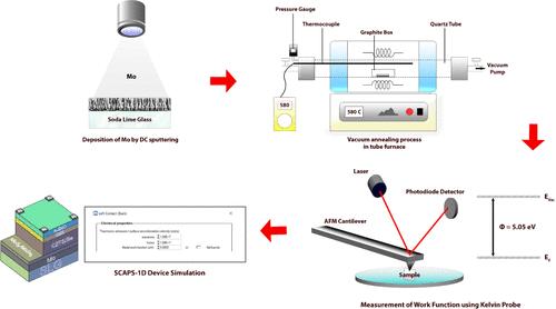
由于钼(Mo)在光吸收层沉积过程中具有热稳定性和在高工作温度下的化学稳定性,因此在以卤化铝为基础的薄膜光伏设备中被用作背电极材料。然而,钼与吸收层之间无意形成的界面层会对设备性能产生不利影响。此外,与其他新出现的 p 型卤化铝吸收层材料的半导体功函数相比,钼的功函数较低,这导致背接触界面的空穴传输过程受到抑制,从而导致开路电压较低。因此,必须努力提高钼薄膜的功函数,以改善器件性能。在这项研究中,研究了在 580 °C 真空条件下进行沉积后热处理对直流溅射钼薄膜的微观结构、电子、电气和形态特性的影响。结果表明,真空退火改善了微观结构特性,从而促进了更好的表面拓扑结构和电子传导机制。更重要的是,真空退火后钼薄膜的功函数提高到了 5.05 eV。在 SCAPS-1D 数值模拟研究中采用了所获得的 5.05 eV 的实验功函数,以突出 Mo 的功函数在减少 MoS2/MoSe2 界面层对 CZTS/CZTSe 器件的开路电压(Voc)、短路电流(Jsc)、填充因子(FF)和效率(PCE)的负面影响方面的关键作用。根据模拟结果,功函数为 4.6 eV 的 Mo(多晶 Mo 的平均值)可使 CZTS 和 CZTSe 器件的效率达到 15%左右,这是与低质量界面层(低载流子迁移率和高缺陷密度)共同作用的结果。然而,功函数为 5.05 eV 的钼使 CZTS 和 CZTSe 器件的效率分别提高了 19% 和 23%。因此,尽管形成了有害的界面层,但增强钼背接触功函数的方法是提高光伏器件整体性能的可行途径。
Revealing the Subtle Role of DC-Sputtered Mo Back Contact Work Function in Mitigating the Detrimental Effects of the MoS2/MoSe2 Interfacial Layer in Kesterite-Based Thin Film Solar Cells
Due to thermal robustness and chemical stability at high working temperatures during photo-absorber layer deposition, molybdenum (Mo) is favored as the back electrode material in chalcogenide-based thin film photovoltaic devices. However, the unintentional formation of an interfacial layer between Mo and the absorber layer adversely affects the deviceperformance. In addition, the lower work function of Mo compared to the semiconductor work function of other emerging p-type chalcogenide absorber layer materials results in low open-circuit voltage caused by the inhibition of the hole-transport process at the back contact interface. Therefore, efforts toward the enhancement of the work function of Mo thin film are imperative to improve the device performance. In this research, the impact of post-deposition heat treatment in vacuum condition at 580 °C on the microstructural, electronic, electrical, and morphological properties of DC-sputtered Mo thin films was studied. It was shown that vacuum annealing improves the microstructural properties, which in turn promotes better surface topology and electron conduction mechanism. More importantly, the work function of the Mo thin film was increased up to 5.05 eV after vacuum annealing. The obtained experimental work function of 5.05 eV was employed in numerical simulation study through SCAPS-1D to highlight the critical role of work function of Mo in reducing the negative impact of the MoS2/MoSe2 interfacial layer in terms of open-circuit voltage (Voc), short-circuit current (Jsc), fill factor (FF), and efficiency (PCE) of CZTS/CZTSe devices. Based on the simulation results, Mo with a work function of 4.6 eV (average for a polycrystalline Mo) results in efficiency of around 15% for both CZTS and CZTSe devices, which was modeled together with low-quality interfacial layer (low carrier mobility and high defect density). However, Mo with a work function of 5.05 eV results in improved efficiency of 19% and 23% for CZTS and CZTSe devices, respectively. Hence, the approach of enhancing the Mo back contact work function is shown as a plausible pathway to enhance the overall performance of the photovoltaic device despite the formation of a detrimental interfacial layer.
期刊介绍:
Energy & Fuels publishes reports of research in the technical area defined by the intersection of the disciplines of chemistry and chemical engineering and the application domain of non-nuclear energy and fuels. This includes research directed at the formation of, exploration for, and production of fossil fuels and biomass; the properties and structure or molecular composition of both raw fuels and refined products; the chemistry involved in the processing and utilization of fuels; fuel cells and their applications; and the analytical and instrumental techniques used in investigations of the foregoing areas.

 求助内容:
求助内容: 应助结果提醒方式:


