Aroop K. Behera, C. Thomas Harris, Douglas V. Pete, Christopher M. Smyth, Marta B. Muniz, Ozhan Koybasi, Takashi Taniguchi, Kenji Watanabe, Branson D. Belle and Suprem R. Das*,
{"title":"一维边缘接触石墨烯异质结构场效应晶体管中由电荷同质性引发的低频噪声","authors":"Aroop K. Behera, C. Thomas Harris, Douglas V. Pete, Christopher M. Smyth, Marta B. Muniz, Ozhan Koybasi, Takashi Taniguchi, Kenji Watanabe, Branson D. Belle and Suprem R. Das*, ","doi":"10.1021/acsanm.4c00367","DOIUrl":null,"url":null,"abstract":"<p >We have previously shown that one-dimensional edge contact to two-dimensional heterostructure field effect transistors with a graphene channel, and hexagonal boron nitride, as both the substrate material and top encapsulated layer, show ultrahigh carrier mobility and ultralow carrier noise (low frequency noise, LFN). Although the noise mechanism of the transistor devices in the ON state was modeled based on microscopic scattering mechanisms caused by charge carriers and phonons, the model was based on normalized noise spectral density following Hooge’s noise model in the ON-state. In this article, we show that the normalized noise current densities within the charge residual region of two similarly fabricated edge-contacted and encapsulated graphene heterostructure field effect transistors show different trends with overdrive voltage that resemble previously reported results in the literature. Here we explain the poorly understood and conflicting LFN trends in the charge residual region (low charge carrier regime) by correlating the spatial charge inhomogeneity near the Dirac point in heterostructure devices to electron–hole puddles. By systematically studying the temperature-dependent transport, LFN and by modeling the channel characteristics in such devices within the charge residual region, we show that the carriers inside electron–hole puddles get pinned at lower temperatures and unpinned at higher temperatures, as consistently shown in their normalized flat-band spectral variation as a function of overdrive voltage. More generally, near the charge neutrality region of single-layer graphene devices, the LFN is described by a correlated carrier number and mobility fluctuations of the charge carriers. Understanding the carrier physics in encapsulated high-performance and edge-contacted heterostructure two-dimensional devices will aid us in not only engineering low-noise graphene-based FETs for future digital and analog electronics but also understanding the noise associated with Dirac-type materials.</p>","PeriodicalId":6,"journal":{"name":"ACS Applied Nano Materials","volume":"7 11","pages":"12366–12375"},"PeriodicalIF":5.5000,"publicationDate":"2024-05-16","publicationTypes":"Journal Article","fieldsOfStudy":null,"isOpenAccess":false,"openAccessPdf":"","citationCount":"0","resultStr":"{\"title\":\"Charge-Inhomogeneity-Mediated Low-Frequency Noise in One-Dimensional Edge-Contacted Graphene Heterostructure Field Effect Transistors\",\"authors\":\"Aroop K. Behera, C. Thomas Harris, Douglas V. Pete, Christopher M. Smyth, Marta B. Muniz, Ozhan Koybasi, Takashi Taniguchi, Kenji Watanabe, Branson D. Belle and Suprem R. Das*, \",\"doi\":\"10.1021/acsanm.4c00367\",\"DOIUrl\":null,\"url\":null,\"abstract\":\"<p >We have previously shown that one-dimensional edge contact to two-dimensional heterostructure field effect transistors with a graphene channel, and hexagonal boron nitride, as both the substrate material and top encapsulated layer, show ultrahigh carrier mobility and ultralow carrier noise (low frequency noise, LFN). Although the noise mechanism of the transistor devices in the ON state was modeled based on microscopic scattering mechanisms caused by charge carriers and phonons, the model was based on normalized noise spectral density following Hooge’s noise model in the ON-state. In this article, we show that the normalized noise current densities within the charge residual region of two similarly fabricated edge-contacted and encapsulated graphene heterostructure field effect transistors show different trends with overdrive voltage that resemble previously reported results in the literature. Here we explain the poorly understood and conflicting LFN trends in the charge residual region (low charge carrier regime) by correlating the spatial charge inhomogeneity near the Dirac point in heterostructure devices to electron–hole puddles. By systematically studying the temperature-dependent transport, LFN and by modeling the channel characteristics in such devices within the charge residual region, we show that the carriers inside electron–hole puddles get pinned at lower temperatures and unpinned at higher temperatures, as consistently shown in their normalized flat-band spectral variation as a function of overdrive voltage. More generally, near the charge neutrality region of single-layer graphene devices, the LFN is described by a correlated carrier number and mobility fluctuations of the charge carriers. Understanding the carrier physics in encapsulated high-performance and edge-contacted heterostructure two-dimensional devices will aid us in not only engineering low-noise graphene-based FETs for future digital and analog electronics but also understanding the noise associated with Dirac-type materials.</p>\",\"PeriodicalId\":6,\"journal\":{\"name\":\"ACS Applied Nano Materials\",\"volume\":\"7 11\",\"pages\":\"12366–12375\"},\"PeriodicalIF\":5.5000,\"publicationDate\":\"2024-05-16\",\"publicationTypes\":\"Journal Article\",\"fieldsOfStudy\":null,\"isOpenAccess\":false,\"openAccessPdf\":\"\",\"citationCount\":\"0\",\"resultStr\":null,\"platform\":\"Semanticscholar\",\"paperid\":null,\"PeriodicalName\":\"ACS Applied Nano Materials\",\"FirstCategoryId\":\"88\",\"ListUrlMain\":\"https://pubs.acs.org/doi/10.1021/acsanm.4c00367\",\"RegionNum\":2,\"RegionCategory\":\"材料科学\",\"ArticlePicture\":[],\"TitleCN\":null,\"AbstractTextCN\":null,\"PMCID\":null,\"EPubDate\":\"\",\"PubModel\":\"\",\"JCR\":\"Q2\",\"JCRName\":\"MATERIALS SCIENCE, MULTIDISCIPLINARY\",\"Score\":null,\"Total\":0}","platform":"Semanticscholar","paperid":null,"PeriodicalName":"ACS Applied Nano Materials","FirstCategoryId":"88","ListUrlMain":"https://pubs.acs.org/doi/10.1021/acsanm.4c00367","RegionNum":2,"RegionCategory":"材料科学","ArticlePicture":[],"TitleCN":null,"AbstractTextCN":null,"PMCID":null,"EPubDate":"","PubModel":"","JCR":"Q2","JCRName":"MATERIALS SCIENCE, MULTIDISCIPLINARY","Score":null,"Total":0}
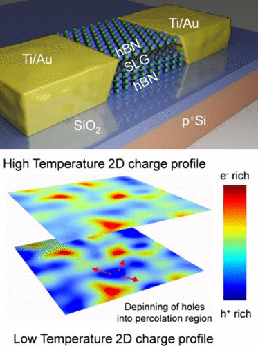
Charge-Inhomogeneity-Mediated Low-Frequency Noise in One-Dimensional Edge-Contacted Graphene Heterostructure Field Effect Transistors
We have previously shown that one-dimensional edge contact to two-dimensional heterostructure field effect transistors with a graphene channel, and hexagonal boron nitride, as both the substrate material and top encapsulated layer, show ultrahigh carrier mobility and ultralow carrier noise (low frequency noise, LFN). Although the noise mechanism of the transistor devices in the ON state was modeled based on microscopic scattering mechanisms caused by charge carriers and phonons, the model was based on normalized noise spectral density following Hooge’s noise model in the ON-state. In this article, we show that the normalized noise current densities within the charge residual region of two similarly fabricated edge-contacted and encapsulated graphene heterostructure field effect transistors show different trends with overdrive voltage that resemble previously reported results in the literature. Here we explain the poorly understood and conflicting LFN trends in the charge residual region (low charge carrier regime) by correlating the spatial charge inhomogeneity near the Dirac point in heterostructure devices to electron–hole puddles. By systematically studying the temperature-dependent transport, LFN and by modeling the channel characteristics in such devices within the charge residual region, we show that the carriers inside electron–hole puddles get pinned at lower temperatures and unpinned at higher temperatures, as consistently shown in their normalized flat-band spectral variation as a function of overdrive voltage. More generally, near the charge neutrality region of single-layer graphene devices, the LFN is described by a correlated carrier number and mobility fluctuations of the charge carriers. Understanding the carrier physics in encapsulated high-performance and edge-contacted heterostructure two-dimensional devices will aid us in not only engineering low-noise graphene-based FETs for future digital and analog electronics but also understanding the noise associated with Dirac-type materials.
期刊介绍:
ACS Applied Nano Materials is an interdisciplinary journal publishing original research covering all aspects of engineering, chemistry, physics and biology relevant to applications of nanomaterials. The journal is devoted to reports of new and original experimental and theoretical research of an applied nature that integrate knowledge in the areas of materials, engineering, physics, bioscience, and chemistry into important applications of nanomaterials.


 求助内容:
求助内容: 应助结果提醒方式:


