Yuhan Du, Xingchen Ji, Weiqiang Xie, Yu He, Yong Zhang, Meng Tian, Yikai Su
{"title":"用于近紫外集成光子学的高效光纤芯片边缘耦合器","authors":"Yuhan Du, Xingchen Ji, Weiqiang Xie, Yu He, Yong Zhang, Meng Tian, Yikai Su","doi":"10.1002/admt.202400196","DOIUrl":null,"url":null,"abstract":"<p>Integrated photonics is demanded in applications operating at ultraviolet to visible wavelengths, such as atomic/quantum systems, on-chip broadband receivers, and far-field structured illumination autofluorescence microscopy. A fundamental challenge in these applications is efficient edge coupling from a single-mode fiber (SMF) to on-chip photonic components, which is critical for on-chip integration. In this paper, a high-efficiency edge coupler based on an alumina-on-insulator platform is introduced and experimentally validated. The coupler employs a symmetric double-tip taper and a multimode interference (MMI)-based optical combiner. The double-tip taper effectively expands the mode field diameter at the chip facet to match that of the SMF at the initial stage. Then the MMI-based combiner efficiently combines the two channels in the taper into a highly confined strip waveguide. A coupling loss of 2.85 dB/facet has been achieved for the transverse magnetic mode at the wavelength of 407 nm, which is the lowest insertion loss for fiber-chip coupling on this platform to the best of the knowledge. The design can significantly reduce the insertion loss associated with fiber-chip coupling, offering a key component for diverse areas ranging from atomic/quantum photonic integrated circuits and ultra-high capacity communications to optical microscopes.</p>","PeriodicalId":7292,"journal":{"name":"Advanced Materials Technologies","volume":null,"pages":null},"PeriodicalIF":6.4000,"publicationDate":"2024-05-16","publicationTypes":"Journal Article","fieldsOfStudy":null,"isOpenAccess":false,"openAccessPdf":"","citationCount":"0","resultStr":"{\"title\":\"High-Efficiency Fiber-Chip Edge Coupler for Near-Ultraviolet Integrated Photonics\",\"authors\":\"Yuhan Du, Xingchen Ji, Weiqiang Xie, Yu He, Yong Zhang, Meng Tian, Yikai Su\",\"doi\":\"10.1002/admt.202400196\",\"DOIUrl\":null,\"url\":null,\"abstract\":\"<p>Integrated photonics is demanded in applications operating at ultraviolet to visible wavelengths, such as atomic/quantum systems, on-chip broadband receivers, and far-field structured illumination autofluorescence microscopy. A fundamental challenge in these applications is efficient edge coupling from a single-mode fiber (SMF) to on-chip photonic components, which is critical for on-chip integration. In this paper, a high-efficiency edge coupler based on an alumina-on-insulator platform is introduced and experimentally validated. The coupler employs a symmetric double-tip taper and a multimode interference (MMI)-based optical combiner. The double-tip taper effectively expands the mode field diameter at the chip facet to match that of the SMF at the initial stage. Then the MMI-based combiner efficiently combines the two channels in the taper into a highly confined strip waveguide. A coupling loss of 2.85 dB/facet has been achieved for the transverse magnetic mode at the wavelength of 407 nm, which is the lowest insertion loss for fiber-chip coupling on this platform to the best of the knowledge. The design can significantly reduce the insertion loss associated with fiber-chip coupling, offering a key component for diverse areas ranging from atomic/quantum photonic integrated circuits and ultra-high capacity communications to optical microscopes.</p>\",\"PeriodicalId\":7292,\"journal\":{\"name\":\"Advanced Materials Technologies\",\"volume\":null,\"pages\":null},\"PeriodicalIF\":6.4000,\"publicationDate\":\"2024-05-16\",\"publicationTypes\":\"Journal Article\",\"fieldsOfStudy\":null,\"isOpenAccess\":false,\"openAccessPdf\":\"\",\"citationCount\":\"0\",\"resultStr\":null,\"platform\":\"Semanticscholar\",\"paperid\":null,\"PeriodicalName\":\"Advanced Materials Technologies\",\"FirstCategoryId\":\"88\",\"ListUrlMain\":\"https://onlinelibrary.wiley.com/doi/10.1002/admt.202400196\",\"RegionNum\":3,\"RegionCategory\":\"材料科学\",\"ArticlePicture\":[],\"TitleCN\":null,\"AbstractTextCN\":null,\"PMCID\":null,\"EPubDate\":\"\",\"PubModel\":\"\",\"JCR\":\"Q1\",\"JCRName\":\"MATERIALS SCIENCE, MULTIDISCIPLINARY\",\"Score\":null,\"Total\":0}","platform":"Semanticscholar","paperid":null,"PeriodicalName":"Advanced Materials Technologies","FirstCategoryId":"88","ListUrlMain":"https://onlinelibrary.wiley.com/doi/10.1002/admt.202400196","RegionNum":3,"RegionCategory":"材料科学","ArticlePicture":[],"TitleCN":null,"AbstractTextCN":null,"PMCID":null,"EPubDate":"","PubModel":"","JCR":"Q1","JCRName":"MATERIALS SCIENCE, MULTIDISCIPLINARY","Score":null,"Total":0}
High-Efficiency Fiber-Chip Edge Coupler for Near-Ultraviolet Integrated Photonics
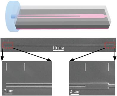
Integrated photonics is demanded in applications operating at ultraviolet to visible wavelengths, such as atomic/quantum systems, on-chip broadband receivers, and far-field structured illumination autofluorescence microscopy. A fundamental challenge in these applications is efficient edge coupling from a single-mode fiber (SMF) to on-chip photonic components, which is critical for on-chip integration. In this paper, a high-efficiency edge coupler based on an alumina-on-insulator platform is introduced and experimentally validated. The coupler employs a symmetric double-tip taper and a multimode interference (MMI)-based optical combiner. The double-tip taper effectively expands the mode field diameter at the chip facet to match that of the SMF at the initial stage. Then the MMI-based combiner efficiently combines the two channels in the taper into a highly confined strip waveguide. A coupling loss of 2.85 dB/facet has been achieved for the transverse magnetic mode at the wavelength of 407 nm, which is the lowest insertion loss for fiber-chip coupling on this platform to the best of the knowledge. The design can significantly reduce the insertion loss associated with fiber-chip coupling, offering a key component for diverse areas ranging from atomic/quantum photonic integrated circuits and ultra-high capacity communications to optical microscopes.
期刊介绍:
Advanced Materials Technologies Advanced Materials Technologies is the new home for all technology-related materials applications research, with particular focus on advanced device design, fabrication and integration, as well as new technologies based on novel materials. It bridges the gap between fundamental laboratory research and industry.

 求助内容:
求助内容: 应助结果提醒方式:


