{"title":"自供电近紫外γ-InSe/石墨烯异质结构光电探测器中的高效载流子倍增,外部量子效率超过 161.","authors":"Yuanzheng Li, Jiayu Pan, Chuxin Yan, Jixiu Li, Wei Xin, Yutong Zhang, Weizhen Liu*, Xinfeng Liu*, Haiyang Xu* and Yichun Liu, ","doi":"10.1021/acs.nanolett.4c01238","DOIUrl":null,"url":null,"abstract":"<p >Carrier multiplication (CM) in semiconductors, the process of absorbing a single high-energy photon to form two or more electron–hole pairs, offers great potential for the high-response detection of high-energy photons in the ultraviolet spectrum. However, compared to two-dimensional semiconductors, conventional bulk semiconductors not only face integration and flexibility bottlenecks but also exhibit inferior CM performance. To attain efficient CM for ultraviolet detection, we designed a two-terminal photodetector featuring a unilateral Schottky junction based on a two-dimensional γ-InSe/graphene heterostructure. Benefiting from a strong built-in electric field, the photogenerated high-energy electrons in γ-InSe, an ideal ultraviolet light-absorbing layer, can efficiently transfer to graphene without cooling. It results in efficient CM within the graphene, yielding an ultrahigh responsivity of 468 mA/W and a record-high external quantum efficiency of 161.2% when it is exposed to 360 nm light at zero bias. This work provides valuable insights into developing next-generation ultraviolet photodetectors with high performance and low-power consumption.</p>","PeriodicalId":53,"journal":{"name":"Nano Letters","volume":"24 24","pages":"7252–7260"},"PeriodicalIF":9.1000,"publicationDate":"2024-05-16","publicationTypes":"Journal Article","fieldsOfStudy":null,"isOpenAccess":false,"openAccessPdf":"","citationCount":"0","resultStr":"{\"title\":\"Efficient Carrier Multiplication in Self-Powered Near-Ultraviolet γ-InSe/Graphene Heterostructure Photodetector with External Quantum Efficiency Exceeding 161%\",\"authors\":\"Yuanzheng Li, Jiayu Pan, Chuxin Yan, Jixiu Li, Wei Xin, Yutong Zhang, Weizhen Liu*, Xinfeng Liu*, Haiyang Xu* and Yichun Liu, \",\"doi\":\"10.1021/acs.nanolett.4c01238\",\"DOIUrl\":null,\"url\":null,\"abstract\":\"<p >Carrier multiplication (CM) in semiconductors, the process of absorbing a single high-energy photon to form two or more electron–hole pairs, offers great potential for the high-response detection of high-energy photons in the ultraviolet spectrum. However, compared to two-dimensional semiconductors, conventional bulk semiconductors not only face integration and flexibility bottlenecks but also exhibit inferior CM performance. To attain efficient CM for ultraviolet detection, we designed a two-terminal photodetector featuring a unilateral Schottky junction based on a two-dimensional γ-InSe/graphene heterostructure. Benefiting from a strong built-in electric field, the photogenerated high-energy electrons in γ-InSe, an ideal ultraviolet light-absorbing layer, can efficiently transfer to graphene without cooling. It results in efficient CM within the graphene, yielding an ultrahigh responsivity of 468 mA/W and a record-high external quantum efficiency of 161.2% when it is exposed to 360 nm light at zero bias. This work provides valuable insights into developing next-generation ultraviolet photodetectors with high performance and low-power consumption.</p>\",\"PeriodicalId\":53,\"journal\":{\"name\":\"Nano Letters\",\"volume\":\"24 24\",\"pages\":\"7252–7260\"},\"PeriodicalIF\":9.1000,\"publicationDate\":\"2024-05-16\",\"publicationTypes\":\"Journal Article\",\"fieldsOfStudy\":null,\"isOpenAccess\":false,\"openAccessPdf\":\"\",\"citationCount\":\"0\",\"resultStr\":null,\"platform\":\"Semanticscholar\",\"paperid\":null,\"PeriodicalName\":\"Nano Letters\",\"FirstCategoryId\":\"88\",\"ListUrlMain\":\"https://pubs.acs.org/doi/10.1021/acs.nanolett.4c01238\",\"RegionNum\":1,\"RegionCategory\":\"材料科学\",\"ArticlePicture\":[],\"TitleCN\":null,\"AbstractTextCN\":null,\"PMCID\":null,\"EPubDate\":\"\",\"PubModel\":\"\",\"JCR\":\"Q1\",\"JCRName\":\"CHEMISTRY, MULTIDISCIPLINARY\",\"Score\":null,\"Total\":0}","platform":"Semanticscholar","paperid":null,"PeriodicalName":"Nano Letters","FirstCategoryId":"88","ListUrlMain":"https://pubs.acs.org/doi/10.1021/acs.nanolett.4c01238","RegionNum":1,"RegionCategory":"材料科学","ArticlePicture":[],"TitleCN":null,"AbstractTextCN":null,"PMCID":null,"EPubDate":"","PubModel":"","JCR":"Q1","JCRName":"CHEMISTRY, MULTIDISCIPLINARY","Score":null,"Total":0}
引用次数: 0
摘要
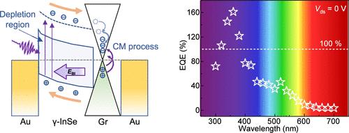
半导体中的载流子倍增(CM)是吸收单个高能光子形成两个或多个电子-空穴对的过程,它为紫外光谱中高能光子的高响应检测提供了巨大的潜力。然而,与二维半导体相比,传统的体半导体不仅在集成度和灵活性方面存在瓶颈,而且 CM 性能也较差。为了实现紫外探测的高效 CM,我们设计了一种双端光电探测器,其特点是基于二维γ-InSe/石墨烯异质结构的单边肖特基结。得益于强大的内置电场,γ-InSe(理想的紫外线吸收层)中光生成的高能电子无需冷却即可高效地转移到石墨烯中。这使得石墨烯内部产生了高效的CM,当石墨烯在零偏压下暴露在360纳米的光线下时,产生了468 mA/W的超高响应率和161.2%的创纪录高外部量子效率。这项工作为开发高性能、低功耗的下一代紫外线光电探测器提供了宝贵的见解。
Efficient Carrier Multiplication in Self-Powered Near-Ultraviolet γ-InSe/Graphene Heterostructure Photodetector with External Quantum Efficiency Exceeding 161%
Carrier multiplication (CM) in semiconductors, the process of absorbing a single high-energy photon to form two or more electron–hole pairs, offers great potential for the high-response detection of high-energy photons in the ultraviolet spectrum. However, compared to two-dimensional semiconductors, conventional bulk semiconductors not only face integration and flexibility bottlenecks but also exhibit inferior CM performance. To attain efficient CM for ultraviolet detection, we designed a two-terminal photodetector featuring a unilateral Schottky junction based on a two-dimensional γ-InSe/graphene heterostructure. Benefiting from a strong built-in electric field, the photogenerated high-energy electrons in γ-InSe, an ideal ultraviolet light-absorbing layer, can efficiently transfer to graphene without cooling. It results in efficient CM within the graphene, yielding an ultrahigh responsivity of 468 mA/W and a record-high external quantum efficiency of 161.2% when it is exposed to 360 nm light at zero bias. This work provides valuable insights into developing next-generation ultraviolet photodetectors with high performance and low-power consumption.
期刊介绍:
Nano Letters serves as a dynamic platform for promptly disseminating original results in fundamental, applied, and emerging research across all facets of nanoscience and nanotechnology. A pivotal criterion for inclusion within Nano Letters is the convergence of at least two different areas or disciplines, ensuring a rich interdisciplinary scope. The journal is dedicated to fostering exploration in diverse areas, including:
- Experimental and theoretical findings on physical, chemical, and biological phenomena at the nanoscale
- Synthesis, characterization, and processing of organic, inorganic, polymer, and hybrid nanomaterials through physical, chemical, and biological methodologies
- Modeling and simulation of synthetic, assembly, and interaction processes
- Realization of integrated nanostructures and nano-engineered devices exhibiting advanced performance
- Applications of nanoscale materials in living and environmental systems
Nano Letters is committed to advancing and showcasing groundbreaking research that intersects various domains, fostering innovation and collaboration in the ever-evolving field of nanoscience and nanotechnology.


 求助内容:
求助内容: 应助结果提醒方式:


