通过操纵界面层实现可偏置开关的双模有机光电二极管

IF 18.5 1区 材料科学 Q1 CHEMISTRY, MULTIDISCIPLINARY
Jianhua Xiao, Jiaao Wu, Fangchen Zhu, Jiehao Ke, Qingxia Liu, Yang Wang, Liu Yuan, Huiling Tai, Yadong Jiang
{"title":"通过操纵界面层实现可偏置开关的双模有机光电二极管","authors":"Jianhua Xiao, Jiaao Wu, Fangchen Zhu, Jiehao Ke, Qingxia Liu, Yang Wang, Liu Yuan, Huiling Tai, Yadong Jiang","doi":"10.1002/adfm.202404711","DOIUrl":null,"url":null,"abstract":"Bias-switchable dual-mode organic photodiodes (OPDs) that integrate photovoltaic and photomultiplication modes are recently developed and shown prospects in complex light-intensity applications. Yet, the device physics that focuses on carrier dynamics is still a challenge and needs to be further explored. Herein, dual-mode OPDs are developed through interface layer manipulation, that is, introducing cathode interface layers (typically, Zn<sub>x</sub>O:D149) with deep energy levels and abundant bulk defects and an anode interface layer of thermally-evaporated ZnO (e-ZnO) with a wide bandgap. Under reverse bias, Zn<sub>x</sub>O:D149 forms a barrier wall to effectively block external holes and maintain the photovoltaic mode of the OPDs. Under forward bias, the capturing effect of Zn<sub>x</sub>O:D149 and blocking effect of e-ZnO help to reduce the dark current; when under illumination, defect traps capture photo-generated holes, eliminating the barrier traps and promoting unobstructed injection of external carriers to achieve photomultiplication effect. The typical device delivers high specific detectivity (&gt;10<sup>12</sup> Jones) and fast response (&lt;40 µs), and exhibits disparate external quantum efficiency in two operating modes, showing promise for simultaneously detecting faint and strong light. This general strategy for preparing dual-mode OPDs is compatible with CMOS processing technology and meets the miniaturization and integration requirements of next-generation detection systems.","PeriodicalId":112,"journal":{"name":"Advanced Functional Materials","volume":null,"pages":null},"PeriodicalIF":18.5000,"publicationDate":"2024-05-14","publicationTypes":"Journal Article","fieldsOfStudy":null,"isOpenAccess":false,"openAccessPdf":"","citationCount":"0","resultStr":"{\"title\":\"Bias-Switchable Dual-Mode Organic Photodiodes Enabled by Manipulation of Interface Layers\",\"authors\":\"Jianhua Xiao, Jiaao Wu, Fangchen Zhu, Jiehao Ke, Qingxia Liu, Yang Wang, Liu Yuan, Huiling Tai, Yadong Jiang\",\"doi\":\"10.1002/adfm.202404711\",\"DOIUrl\":null,\"url\":null,\"abstract\":\"Bias-switchable dual-mode organic photodiodes (OPDs) that integrate photovoltaic and photomultiplication modes are recently developed and shown prospects in complex light-intensity applications. Yet, the device physics that focuses on carrier dynamics is still a challenge and needs to be further explored. Herein, dual-mode OPDs are developed through interface layer manipulation, that is, introducing cathode interface layers (typically, Zn<sub>x</sub>O:D149) with deep energy levels and abundant bulk defects and an anode interface layer of thermally-evaporated ZnO (e-ZnO) with a wide bandgap. Under reverse bias, Zn<sub>x</sub>O:D149 forms a barrier wall to effectively block external holes and maintain the photovoltaic mode of the OPDs. Under forward bias, the capturing effect of Zn<sub>x</sub>O:D149 and blocking effect of e-ZnO help to reduce the dark current; when under illumination, defect traps capture photo-generated holes, eliminating the barrier traps and promoting unobstructed injection of external carriers to achieve photomultiplication effect. The typical device delivers high specific detectivity (&gt;10<sup>12</sup> Jones) and fast response (&lt;40 µs), and exhibits disparate external quantum efficiency in two operating modes, showing promise for simultaneously detecting faint and strong light. This general strategy for preparing dual-mode OPDs is compatible with CMOS processing technology and meets the miniaturization and integration requirements of next-generation detection systems.\",\"PeriodicalId\":112,\"journal\":{\"name\":\"Advanced Functional Materials\",\"volume\":null,\"pages\":null},\"PeriodicalIF\":18.5000,\"publicationDate\":\"2024-05-14\",\"publicationTypes\":\"Journal Article\",\"fieldsOfStudy\":null,\"isOpenAccess\":false,\"openAccessPdf\":\"\",\"citationCount\":\"0\",\"resultStr\":null,\"platform\":\"Semanticscholar\",\"paperid\":null,\"PeriodicalName\":\"Advanced Functional Materials\",\"FirstCategoryId\":\"88\",\"ListUrlMain\":\"https://doi.org/10.1002/adfm.202404711\",\"RegionNum\":1,\"RegionCategory\":\"材料科学\",\"ArticlePicture\":[],\"TitleCN\":null,\"AbstractTextCN\":null,\"PMCID\":null,\"EPubDate\":\"\",\"PubModel\":\"\",\"JCR\":\"Q1\",\"JCRName\":\"CHEMISTRY, MULTIDISCIPLINARY\",\"Score\":null,\"Total\":0}","platform":"Semanticscholar","paperid":null,"PeriodicalName":"Advanced Functional Materials","FirstCategoryId":"88","ListUrlMain":"https://doi.org/10.1002/adfm.202404711","RegionNum":1,"RegionCategory":"材料科学","ArticlePicture":[],"TitleCN":null,"AbstractTextCN":null,"PMCID":null,"EPubDate":"","PubModel":"","JCR":"Q1","JCRName":"CHEMISTRY, MULTIDISCIPLINARY","Score":null,"Total":0}
引用次数: 0

摘要

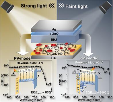
集成了光生伏打和光电倍增模式的偏置可切换双模有机光电二极管(OPD)是最近开发出来的,并在复杂光强的应用中展现出广阔的前景。然而,以载流子动力学为重点的器件物理学仍是一个挑战,需要进一步探索。本文通过界面层操作开发了双模 OPD,即引入具有深能级和丰富体缺陷的阴极界面层(通常为 ZnxO:D149)和具有宽带隙的热蒸发 ZnO(e-ZnO)阳极界面层。在反向偏压下,ZnxO:D149 形成阻挡壁,有效阻挡外部空穴,维持 OPD 的光电模式。在正向偏压下,ZnxO:D149 的捕获效应和 e-ZnO 的阻挡效应有助于降低暗电流;在光照下,缺陷陷阱捕获光生空穴,消除势垒陷阱,促进外部载流子的无障碍注入,从而实现光电倍增效应。这种典型器件具有高比特检测率(1012 琼斯)和快速响应(40 微秒),并在两种工作模式下表现出不同的外部量子效率,显示出同时检测微弱光和强光的前景。这种制备双模式 OPD 的一般策略与 CMOS 处理技术兼容,符合下一代探测系统的微型化和集成化要求。
本文章由计算机程序翻译,如有差异,请以英文原文为准。

Bias-Switchable Dual-Mode Organic Photodiodes Enabled by Manipulation of Interface Layers

Bias-Switchable Dual-Mode Organic Photodiodes Enabled by Manipulation of Interface Layers
Bias-switchable dual-mode organic photodiodes (OPDs) that integrate photovoltaic and photomultiplication modes are recently developed and shown prospects in complex light-intensity applications. Yet, the device physics that focuses on carrier dynamics is still a challenge and needs to be further explored. Herein, dual-mode OPDs are developed through interface layer manipulation, that is, introducing cathode interface layers (typically, ZnxO:D149) with deep energy levels and abundant bulk defects and an anode interface layer of thermally-evaporated ZnO (e-ZnO) with a wide bandgap. Under reverse bias, ZnxO:D149 forms a barrier wall to effectively block external holes and maintain the photovoltaic mode of the OPDs. Under forward bias, the capturing effect of ZnxO:D149 and blocking effect of e-ZnO help to reduce the dark current; when under illumination, defect traps capture photo-generated holes, eliminating the barrier traps and promoting unobstructed injection of external carriers to achieve photomultiplication effect. The typical device delivers high specific detectivity (>1012 Jones) and fast response (<40 µs), and exhibits disparate external quantum efficiency in two operating modes, showing promise for simultaneously detecting faint and strong light. This general strategy for preparing dual-mode OPDs is compatible with CMOS processing technology and meets the miniaturization and integration requirements of next-generation detection systems.
求助全文
通过发布文献求助,成功后即可免费获取论文全文。 去求助
来源期刊
Advanced Functional Materials
Advanced Functional Materials 工程技术-材料科学:综合
CiteScore
29.50
自引率
4.20%
发文量
2086
审稿时长
2.1 months
期刊介绍: Firmly established as a top-tier materials science journal, Advanced Functional Materials reports breakthrough research in all aspects of materials science, including nanotechnology, chemistry, physics, and biology every week. Advanced Functional Materials is known for its rapid and fair peer review, quality content, and high impact, making it the first choice of the international materials science community.
×
引用
GB/T 7714-2015
复制
MLA
复制
APA
复制
导出至
BibTeX EndNote RefMan NoteFirst NoteExpress
×
提示
您的信息不完整,为了账户安全,请先补充。
现在去补充
×
提示
您因"违规操作"
具体请查看互助需知
我知道了
×
提示
确定
请完成安全验证×
copy
已复制链接
快去分享给好友吧!
我知道了
右上角分享
点击右上角分享
0
联系我们:info@booksci.cn Book学术提供免费学术资源搜索服务,方便国内外学者检索中英文文献。致力于提供最便捷和优质的服务体验。 Copyright © 2023 布克学术 All rights reserved.
京ICP备2023020795号-1
ghs 京公网安备 11010802042870号
Book学术文献互助
Book学术文献互助群
群 号:481959085
Book学术官方微信