Tianyu Yu , Yunlei Jiang , Suxia Liang , Zhiguo Zhao , Sheng Zou , Jie Su , Renjie Hua , Cang Liang , Wangfan Chen , Mi Zhang , Wenjun Zhang , Lei Shi , Yuan Dong
{"title":"溅射压力对直流磁控溅射沉积的大面积 IWO 薄膜性能的影响","authors":"Tianyu Yu , Yunlei Jiang , Suxia Liang , Zhiguo Zhao , Sheng Zou , Jie Su , Renjie Hua , Cang Liang , Wangfan Chen , Mi Zhang , Wenjun Zhang , Lei Shi , Yuan Dong","doi":"10.1016/j.cap.2024.05.006","DOIUrl":null,"url":null,"abstract":"<div><p>Tungsten doped indium oxide (In<sub>2</sub>O<sub>3</sub>: W, IWO) thin films have been attracting increasing attention due to their excellent optoelectronic properties. Here, a series of IWO thin films were prepared using direct current (DC) magnetron sputtering method, by varying the sputtering pressure. Analysis revealed that the IWO films prepared under sputtering pressure of 0.4 Pa exhibited excellent optoelectronic performance, with low square resistance, resistivity, high carrier concentration and mobility. The resulting semi-transparent perovskite solar cells (ST-PSCs), with IWO fabricated under 0.4 Pa, yield a PCE of 15.71 % for the large area modules of 100 cm<sup>2</sup> (active area 64.8 cm<sup>2</sup>).</p></div>","PeriodicalId":11037,"journal":{"name":"Current Applied Physics","volume":null,"pages":null},"PeriodicalIF":2.4000,"publicationDate":"2024-05-08","publicationTypes":"Journal Article","fieldsOfStudy":null,"isOpenAccess":false,"openAccessPdf":"","citationCount":"0","resultStr":"{\"title\":\"Effect of sputtering pressure on the properties of large area IWO thin films deposited by direct current magnetron sputtering\",\"authors\":\"Tianyu Yu , Yunlei Jiang , Suxia Liang , Zhiguo Zhao , Sheng Zou , Jie Su , Renjie Hua , Cang Liang , Wangfan Chen , Mi Zhang , Wenjun Zhang , Lei Shi , Yuan Dong\",\"doi\":\"10.1016/j.cap.2024.05.006\",\"DOIUrl\":null,\"url\":null,\"abstract\":\"<div><p>Tungsten doped indium oxide (In<sub>2</sub>O<sub>3</sub>: W, IWO) thin films have been attracting increasing attention due to their excellent optoelectronic properties. Here, a series of IWO thin films were prepared using direct current (DC) magnetron sputtering method, by varying the sputtering pressure. Analysis revealed that the IWO films prepared under sputtering pressure of 0.4 Pa exhibited excellent optoelectronic performance, with low square resistance, resistivity, high carrier concentration and mobility. The resulting semi-transparent perovskite solar cells (ST-PSCs), with IWO fabricated under 0.4 Pa, yield a PCE of 15.71 % for the large area modules of 100 cm<sup>2</sup> (active area 64.8 cm<sup>2</sup>).</p></div>\",\"PeriodicalId\":11037,\"journal\":{\"name\":\"Current Applied Physics\",\"volume\":null,\"pages\":null},\"PeriodicalIF\":2.4000,\"publicationDate\":\"2024-05-08\",\"publicationTypes\":\"Journal Article\",\"fieldsOfStudy\":null,\"isOpenAccess\":false,\"openAccessPdf\":\"\",\"citationCount\":\"0\",\"resultStr\":null,\"platform\":\"Semanticscholar\",\"paperid\":null,\"PeriodicalName\":\"Current Applied Physics\",\"FirstCategoryId\":\"101\",\"ListUrlMain\":\"https://www.sciencedirect.com/science/article/pii/S1567173924000956\",\"RegionNum\":4,\"RegionCategory\":\"物理与天体物理\",\"ArticlePicture\":[],\"TitleCN\":null,\"AbstractTextCN\":null,\"PMCID\":null,\"EPubDate\":\"\",\"PubModel\":\"\",\"JCR\":\"Q3\",\"JCRName\":\"MATERIALS SCIENCE, MULTIDISCIPLINARY\",\"Score\":null,\"Total\":0}","platform":"Semanticscholar","paperid":null,"PeriodicalName":"Current Applied Physics","FirstCategoryId":"101","ListUrlMain":"https://www.sciencedirect.com/science/article/pii/S1567173924000956","RegionNum":4,"RegionCategory":"物理与天体物理","ArticlePicture":[],"TitleCN":null,"AbstractTextCN":null,"PMCID":null,"EPubDate":"","PubModel":"","JCR":"Q3","JCRName":"MATERIALS SCIENCE, MULTIDISCIPLINARY","Score":null,"Total":0}
引用次数: 0
摘要
掺杂钨的氧化铟(In2O3: W,IWO)薄膜因其卓越的光电特性而受到越来越多的关注。本文采用直流(DC)磁控溅射法,通过改变溅射压力制备了一系列 IWO 薄膜。分析表明,在 0.4 Pa 的溅射压力下制备的 IWO 薄膜具有优异的光电性能,方阻、电阻率低,载流子浓度和迁移率高。在 0.4 Pa 的溅射压力下制备的 IWO 所产生的半透明过氧化物太阳能电池(ST-PSCs),在 100 平方厘米(有效面积 64.8 平方厘米)的大面积模块中,PCE 为 15.71%。
Effect of sputtering pressure on the properties of large area IWO thin films deposited by direct current magnetron sputtering
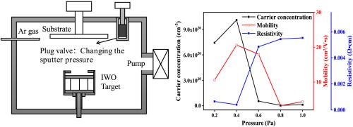
Tungsten doped indium oxide (In2O3: W, IWO) thin films have been attracting increasing attention due to their excellent optoelectronic properties. Here, a series of IWO thin films were prepared using direct current (DC) magnetron sputtering method, by varying the sputtering pressure. Analysis revealed that the IWO films prepared under sputtering pressure of 0.4 Pa exhibited excellent optoelectronic performance, with low square resistance, resistivity, high carrier concentration and mobility. The resulting semi-transparent perovskite solar cells (ST-PSCs), with IWO fabricated under 0.4 Pa, yield a PCE of 15.71 % for the large area modules of 100 cm2 (active area 64.8 cm2).
期刊介绍:
Current Applied Physics (Curr. Appl. Phys.) is a monthly published international journal covering all the fields of applied science investigating the physics of the advanced materials for future applications.
Other areas covered: Experimental and theoretical aspects of advanced materials and devices dealing with synthesis or structural chemistry, physical and electronic properties, photonics, engineering applications, and uniquely pertinent measurement or analytical techniques.
Current Applied Physics, published since 2001, covers physics, chemistry and materials science, including bio-materials, with their engineering aspects. It is a truly interdisciplinary journal opening a forum for scientists of all related fields, a unique point of the journal discriminating it from other worldwide and/or Pacific Rim applied physics journals.
Regular research papers, letters and review articles with contents meeting the scope of the journal will be considered for publication after peer review.
The Journal is owned by the Korean Physical Society.