Jessica Haglund, Takanori Mimura, Jon F. Ihlefeld and John F. Conley Jr.*,
{"title":"工作中的 TaN/Hf0.5Zr0.5O2/TaN 金属/铁电/金属 (MFM) 器件中界面能垒的内部光发射光谱测量结果","authors":"Jessica Haglund, Takanori Mimura, Jon F. Ihlefeld and John F. Conley Jr.*, ","doi":"10.1021/acsaelm.4c00073","DOIUrl":null,"url":null,"abstract":"<p >The effect of the “waking” and subsequent “poling” operations on the electron barriers at both top and bottom electrode interfaces in operating ferroelectric hafnium zirconium oxide (Hf<sub>0.5</sub>Zr<sub>0.5</sub>O<sub>2</sub>, HZO) metal/ferroelectric/metal (MFM) devices are measured for the first time via internal photoemission (IPE) spectroscopy. Top and bottom (TaN/HZO and HZO/TaN) barriers for pristine devices were measured at 2.6 and 2.9 eV, respectively. The waking operation (10 kHz bipolar voltage cycling above the coercive field) increased the top barrier to 2.8 eV while leaving the bottom barrier essentially unchanged. Poling operations (application of a longer 10 ms unipolar pulse) were found to significantly decrease both top and bottom barriers. The poling direction (polarity) had relatively little impact. The barrier for the top interface under positive (P↓) and negative poling (P↑) was 2.1 and 2.2 eV, respectively, while the bottom barrier was 2.3 eV for P↓ and 2.4 eV for P↑. All barrier heights remained unchanged after several months at room temperature. Potential physical mechanisms responsible for the changes observed under electrical operation are consistent with movement and/or creation of charged oxygen vacancy defects.</p>","PeriodicalId":3,"journal":{"name":"ACS Applied Electronic Materials","volume":"6 5","pages":"3249–3256"},"PeriodicalIF":4.7000,"publicationDate":"2024-04-30","publicationTypes":"Journal Article","fieldsOfStudy":null,"isOpenAccess":false,"openAccessPdf":"","citationCount":"0","resultStr":"{\"title\":\"Internal Photoemission Spectroscopy Measurements of Interfacial Energy Barriers in Operating TaN/Hf0.5Zr0.5O2/TaN Metal/Ferroelectric/Metal (MFM) Devices\",\"authors\":\"Jessica Haglund, Takanori Mimura, Jon F. Ihlefeld and John F. Conley Jr.*, \",\"doi\":\"10.1021/acsaelm.4c00073\",\"DOIUrl\":null,\"url\":null,\"abstract\":\"<p >The effect of the “waking” and subsequent “poling” operations on the electron barriers at both top and bottom electrode interfaces in operating ferroelectric hafnium zirconium oxide (Hf<sub>0.5</sub>Zr<sub>0.5</sub>O<sub>2</sub>, HZO) metal/ferroelectric/metal (MFM) devices are measured for the first time via internal photoemission (IPE) spectroscopy. Top and bottom (TaN/HZO and HZO/TaN) barriers for pristine devices were measured at 2.6 and 2.9 eV, respectively. The waking operation (10 kHz bipolar voltage cycling above the coercive field) increased the top barrier to 2.8 eV while leaving the bottom barrier essentially unchanged. Poling operations (application of a longer 10 ms unipolar pulse) were found to significantly decrease both top and bottom barriers. The poling direction (polarity) had relatively little impact. The barrier for the top interface under positive (P↓) and negative poling (P↑) was 2.1 and 2.2 eV, respectively, while the bottom barrier was 2.3 eV for P↓ and 2.4 eV for P↑. All barrier heights remained unchanged after several months at room temperature. Potential physical mechanisms responsible for the changes observed under electrical operation are consistent with movement and/or creation of charged oxygen vacancy defects.</p>\",\"PeriodicalId\":3,\"journal\":{\"name\":\"ACS Applied Electronic Materials\",\"volume\":\"6 5\",\"pages\":\"3249–3256\"},\"PeriodicalIF\":4.7000,\"publicationDate\":\"2024-04-30\",\"publicationTypes\":\"Journal Article\",\"fieldsOfStudy\":null,\"isOpenAccess\":false,\"openAccessPdf\":\"\",\"citationCount\":\"0\",\"resultStr\":null,\"platform\":\"Semanticscholar\",\"paperid\":null,\"PeriodicalName\":\"ACS Applied Electronic Materials\",\"FirstCategoryId\":\"88\",\"ListUrlMain\":\"https://pubs.acs.org/doi/10.1021/acsaelm.4c00073\",\"RegionNum\":3,\"RegionCategory\":\"材料科学\",\"ArticlePicture\":[],\"TitleCN\":null,\"AbstractTextCN\":null,\"PMCID\":null,\"EPubDate\":\"\",\"PubModel\":\"\",\"JCR\":\"Q1\",\"JCRName\":\"ENGINEERING, ELECTRICAL & ELECTRONIC\",\"Score\":null,\"Total\":0}","platform":"Semanticscholar","paperid":null,"PeriodicalName":"ACS Applied Electronic Materials","FirstCategoryId":"88","ListUrlMain":"https://pubs.acs.org/doi/10.1021/acsaelm.4c00073","RegionNum":3,"RegionCategory":"材料科学","ArticlePicture":[],"TitleCN":null,"AbstractTextCN":null,"PMCID":null,"EPubDate":"","PubModel":"","JCR":"Q1","JCRName":"ENGINEERING, ELECTRICAL & ELECTRONIC","Score":null,"Total":0}
Internal Photoemission Spectroscopy Measurements of Interfacial Energy Barriers in Operating TaN/Hf0.5Zr0.5O2/TaN Metal/Ferroelectric/Metal (MFM) Devices
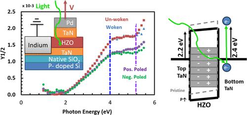
The effect of the “waking” and subsequent “poling” operations on the electron barriers at both top and bottom electrode interfaces in operating ferroelectric hafnium zirconium oxide (Hf0.5Zr0.5O2, HZO) metal/ferroelectric/metal (MFM) devices are measured for the first time via internal photoemission (IPE) spectroscopy. Top and bottom (TaN/HZO and HZO/TaN) barriers for pristine devices were measured at 2.6 and 2.9 eV, respectively. The waking operation (10 kHz bipolar voltage cycling above the coercive field) increased the top barrier to 2.8 eV while leaving the bottom barrier essentially unchanged. Poling operations (application of a longer 10 ms unipolar pulse) were found to significantly decrease both top and bottom barriers. The poling direction (polarity) had relatively little impact. The barrier for the top interface under positive (P↓) and negative poling (P↑) was 2.1 and 2.2 eV, respectively, while the bottom barrier was 2.3 eV for P↓ and 2.4 eV for P↑. All barrier heights remained unchanged after several months at room temperature. Potential physical mechanisms responsible for the changes observed under electrical operation are consistent with movement and/or creation of charged oxygen vacancy defects.
期刊介绍:
ACS Applied Electronic Materials is an interdisciplinary journal publishing original research covering all aspects of electronic materials. The journal is devoted to reports of new and original experimental and theoretical research of an applied nature that integrate knowledge in the areas of materials science, engineering, optics, physics, and chemistry into important applications of electronic materials. Sample research topics that span the journal's scope are inorganic, organic, ionic and polymeric materials with properties that include conducting, semiconducting, superconducting, insulating, dielectric, magnetic, optoelectronic, piezoelectric, ferroelectric and thermoelectric.
Indexed/Abstracted:
Web of Science SCIE
Scopus
CAS
INSPEC
Portico


 求助内容:
求助内容: 应助结果提醒方式:


