Jordan Athas , Joseph Ereifej , Jorge Torres Quiñones, Alexander Abrams, Minhee Yun
{"title":"带有聚二甲基硅氧烷电介质的可扩展顶栅石墨烯场效应晶体管","authors":"Jordan Athas , Joseph Ereifej , Jorge Torres Quiñones, Alexander Abrams, Minhee Yun","doi":"10.1016/j.nwnano.2024.100039","DOIUrl":null,"url":null,"abstract":"<div><p>The limitations of modern CMOS technology have created a call to action for novel devices with great scalability potential. Graphene has been recognized as a suitable material for an enhanced transistor channel based on its incredibly large conductivity while also being easily scaled. Previous research has noted the importance of a top gate device structure, which is difficult to accomplish for graphene transistors due to graphene's incompatibility with oxide growth processes. A novel process flow for graphene field effect transistors with scalability is presented. The emphasis is on the growth of multilayer graphene using chemical vapor deposition and the implementation of polydimethylsiloxane as a gate dielectric. Polydimethylsiloxane gate insulator thickness of 815 nm and 570 nm were successfully developed on 4in large-scale wafers. Two devices of similar channel dimensions and different dielectric were compared and mobilities of 14.57cm<sup>2</sup>V<sup>−1</sup>s<sup>−1</sup> and 0.44 cm<sup>2</sup>V<sup>−1</sup>s<sup>−1</sup> were measured. Gate voltage sweeps from -20 V to 20 V also demonstrated channel current modulation with a charge neutrality point between 5 V and 8 V, indicating achievement of expected device operation.</p></div>","PeriodicalId":100942,"journal":{"name":"Nano Trends","volume":"6 ","pages":"Article 100039"},"PeriodicalIF":0.0000,"publicationDate":"2024-04-15","publicationTypes":"Journal Article","fieldsOfStudy":null,"isOpenAccess":false,"openAccessPdf":"https://www.sciencedirect.com/science/article/pii/S2666978124000102/pdfft?md5=210d0e6eef3d25c7a28cdc23f9c6b2a3&pid=1-s2.0-S2666978124000102-main.pdf","citationCount":"0","resultStr":"{\"title\":\"A scalable top-gate graphene field effect transistor with a polydimethylsiloxane dielectric\",\"authors\":\"Jordan Athas , Joseph Ereifej , Jorge Torres Quiñones, Alexander Abrams, Minhee Yun\",\"doi\":\"10.1016/j.nwnano.2024.100039\",\"DOIUrl\":null,\"url\":null,\"abstract\":\"<div><p>The limitations of modern CMOS technology have created a call to action for novel devices with great scalability potential. Graphene has been recognized as a suitable material for an enhanced transistor channel based on its incredibly large conductivity while also being easily scaled. Previous research has noted the importance of a top gate device structure, which is difficult to accomplish for graphene transistors due to graphene's incompatibility with oxide growth processes. A novel process flow for graphene field effect transistors with scalability is presented. The emphasis is on the growth of multilayer graphene using chemical vapor deposition and the implementation of polydimethylsiloxane as a gate dielectric. Polydimethylsiloxane gate insulator thickness of 815 nm and 570 nm were successfully developed on 4in large-scale wafers. Two devices of similar channel dimensions and different dielectric were compared and mobilities of 14.57cm<sup>2</sup>V<sup>−1</sup>s<sup>−1</sup> and 0.44 cm<sup>2</sup>V<sup>−1</sup>s<sup>−1</sup> were measured. Gate voltage sweeps from -20 V to 20 V also demonstrated channel current modulation with a charge neutrality point between 5 V and 8 V, indicating achievement of expected device operation.</p></div>\",\"PeriodicalId\":100942,\"journal\":{\"name\":\"Nano Trends\",\"volume\":\"6 \",\"pages\":\"Article 100039\"},\"PeriodicalIF\":0.0000,\"publicationDate\":\"2024-04-15\",\"publicationTypes\":\"Journal Article\",\"fieldsOfStudy\":null,\"isOpenAccess\":false,\"openAccessPdf\":\"https://www.sciencedirect.com/science/article/pii/S2666978124000102/pdfft?md5=210d0e6eef3d25c7a28cdc23f9c6b2a3&pid=1-s2.0-S2666978124000102-main.pdf\",\"citationCount\":\"0\",\"resultStr\":null,\"platform\":\"Semanticscholar\",\"paperid\":null,\"PeriodicalName\":\"Nano Trends\",\"FirstCategoryId\":\"1085\",\"ListUrlMain\":\"https://www.sciencedirect.com/science/article/pii/S2666978124000102\",\"RegionNum\":0,\"RegionCategory\":null,\"ArticlePicture\":[],\"TitleCN\":null,\"AbstractTextCN\":null,\"PMCID\":null,\"EPubDate\":\"\",\"PubModel\":\"\",\"JCR\":\"\",\"JCRName\":\"\",\"Score\":null,\"Total\":0}","platform":"Semanticscholar","paperid":null,"PeriodicalName":"Nano Trends","FirstCategoryId":"1085","ListUrlMain":"https://www.sciencedirect.com/science/article/pii/S2666978124000102","RegionNum":0,"RegionCategory":null,"ArticlePicture":[],"TitleCN":null,"AbstractTextCN":null,"PMCID":null,"EPubDate":"","PubModel":"","JCR":"","JCRName":"","Score":null,"Total":0}
引用次数: 0
摘要
现代 CMOS 技术的局限性呼唤具有巨大扩展潜力的新型设备。石墨烯被认为是一种适用于增强型晶体管沟道的材料,因为它具有令人难以置信的高导电率,而且易于扩展。以往的研究已经注意到顶部栅极器件结构的重要性,但由于石墨烯与氧化物生长工艺不相容,石墨烯晶体管很难实现顶部栅极器件结构。本文介绍了具有可扩展性的石墨烯场效应晶体管的新型工艺流程。重点在于使用化学气相沉积法生长多层石墨烯,并使用聚二甲基硅氧烷作为栅极电介质。在 4 英寸大型晶片上成功开发出厚度分别为 815 纳米和 570 纳米的聚二甲基硅氧烷栅极绝缘体。对两个具有相似沟道尺寸和不同电介质的器件进行了比较,测得的迁移率分别为 14.57 cm2V-1s-1 和 0.44 cm2V-1s-1。从 -20 V 到 20 V 的栅极电压扫描也显示了沟道电流调制,电荷中性点在 5 V 到 8 V 之间,表明实现了预期的器件运行。
A scalable top-gate graphene field effect transistor with a polydimethylsiloxane dielectric
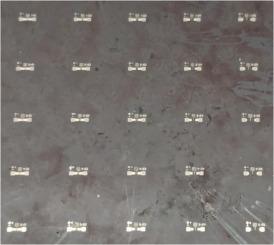
The limitations of modern CMOS technology have created a call to action for novel devices with great scalability potential. Graphene has been recognized as a suitable material for an enhanced transistor channel based on its incredibly large conductivity while also being easily scaled. Previous research has noted the importance of a top gate device structure, which is difficult to accomplish for graphene transistors due to graphene's incompatibility with oxide growth processes. A novel process flow for graphene field effect transistors with scalability is presented. The emphasis is on the growth of multilayer graphene using chemical vapor deposition and the implementation of polydimethylsiloxane as a gate dielectric. Polydimethylsiloxane gate insulator thickness of 815 nm and 570 nm were successfully developed on 4in large-scale wafers. Two devices of similar channel dimensions and different dielectric were compared and mobilities of 14.57cm2V−1s−1 and 0.44 cm2V−1s−1 were measured. Gate voltage sweeps from -20 V to 20 V also demonstrated channel current modulation with a charge neutrality point between 5 V and 8 V, indicating achievement of expected device operation.

 求助内容:
求助内容: 应助结果提醒方式:


