N. V. Bazlov, O. F. Vyvenko, N. V. Niyazova, I. M. Kotina, M. V. Trushin, A. S. Bondarenko
{"title":"硅基氮化铝薄膜的结构和导电性","authors":"N. V. Bazlov, O. F. Vyvenko, N. V. Niyazova, I. M. Kotina, M. V. Trushin, A. S. Bondarenko","doi":"10.1134/S1063774523601260","DOIUrl":null,"url":null,"abstract":"<p>Aluminum nitride films have been synthesized by reactive magnetron sputtering on <i>n</i>-Si(100) substrates. AlN layers with thicknesses from 2 to 150 nm were obtained to establish a correlation between the structure of the films and their electrical conductivity. Electron microscopy revealed that the amorphous structure of the films passes to nanocrystalline one while moving away from the substrate surface. Films with thicknesses below 20 nm had a high conductivity: up to 10 (Ω cm)<sup>–1</sup>; with an increase in thickness the conductivity dropped to 10<sup>–7</sup> (Ω cm)<sup>–1</sup>. The high conductivity of thin AlN layers is believed to be due to the high density of the boundaries of grains built-in into amorphous matrix.</p>","PeriodicalId":527,"journal":{"name":"Crystallography Reports","volume":"69 1","pages":"65 - 72"},"PeriodicalIF":0.6000,"publicationDate":"2024-04-16","publicationTypes":"Journal Article","fieldsOfStudy":null,"isOpenAccess":false,"openAccessPdf":"","citationCount":"0","resultStr":"{\"title\":\"Structure and Electrical Conductivity of Thin AlN Films on Si\",\"authors\":\"N. V. Bazlov, O. F. Vyvenko, N. V. Niyazova, I. M. Kotina, M. V. Trushin, A. S. Bondarenko\",\"doi\":\"10.1134/S1063774523601260\",\"DOIUrl\":null,\"url\":null,\"abstract\":\"<p>Aluminum nitride films have been synthesized by reactive magnetron sputtering on <i>n</i>-Si(100) substrates. AlN layers with thicknesses from 2 to 150 nm were obtained to establish a correlation between the structure of the films and their electrical conductivity. Electron microscopy revealed that the amorphous structure of the films passes to nanocrystalline one while moving away from the substrate surface. Films with thicknesses below 20 nm had a high conductivity: up to 10 (Ω cm)<sup>–1</sup>; with an increase in thickness the conductivity dropped to 10<sup>–7</sup> (Ω cm)<sup>–1</sup>. The high conductivity of thin AlN layers is believed to be due to the high density of the boundaries of grains built-in into amorphous matrix.</p>\",\"PeriodicalId\":527,\"journal\":{\"name\":\"Crystallography Reports\",\"volume\":\"69 1\",\"pages\":\"65 - 72\"},\"PeriodicalIF\":0.6000,\"publicationDate\":\"2024-04-16\",\"publicationTypes\":\"Journal Article\",\"fieldsOfStudy\":null,\"isOpenAccess\":false,\"openAccessPdf\":\"\",\"citationCount\":\"0\",\"resultStr\":null,\"platform\":\"Semanticscholar\",\"paperid\":null,\"PeriodicalName\":\"Crystallography Reports\",\"FirstCategoryId\":\"88\",\"ListUrlMain\":\"https://link.springer.com/article/10.1134/S1063774523601260\",\"RegionNum\":4,\"RegionCategory\":\"材料科学\",\"ArticlePicture\":[],\"TitleCN\":null,\"AbstractTextCN\":null,\"PMCID\":null,\"EPubDate\":\"\",\"PubModel\":\"\",\"JCR\":\"Q4\",\"JCRName\":\"CRYSTALLOGRAPHY\",\"Score\":null,\"Total\":0}","platform":"Semanticscholar","paperid":null,"PeriodicalName":"Crystallography Reports","FirstCategoryId":"88","ListUrlMain":"https://link.springer.com/article/10.1134/S1063774523601260","RegionNum":4,"RegionCategory":"材料科学","ArticlePicture":[],"TitleCN":null,"AbstractTextCN":null,"PMCID":null,"EPubDate":"","PubModel":"","JCR":"Q4","JCRName":"CRYSTALLOGRAPHY","Score":null,"Total":0}
Structure and Electrical Conductivity of Thin AlN Films on Si
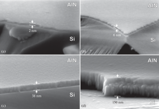
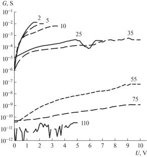
Aluminum nitride films have been synthesized by reactive magnetron sputtering on n-Si(100) substrates. AlN layers with thicknesses from 2 to 150 nm were obtained to establish a correlation between the structure of the films and their electrical conductivity. Electron microscopy revealed that the amorphous structure of the films passes to nanocrystalline one while moving away from the substrate surface. Films with thicknesses below 20 nm had a high conductivity: up to 10 (Ω cm)–1; with an increase in thickness the conductivity dropped to 10–7 (Ω cm)–1. The high conductivity of thin AlN layers is believed to be due to the high density of the boundaries of grains built-in into amorphous matrix.
期刊介绍:
Crystallography Reports is a journal that publishes original articles short communications, and reviews on various aspects of crystallography: diffraction and scattering of X-rays, electrons, and neutrons, determination of crystal structure of inorganic and organic substances, including proteins and other biological substances; UV-VIS and IR spectroscopy; growth, imperfect structure and physical properties of crystals; thin films, liquid crystals, nanomaterials, partially disordered systems, and the methods of studies.
 求助内容:
求助内容: 应助结果提醒方式:


