Issraa Shahine, Quentin Hatte, Maxime Harnois and Pierre-Yves Tessier*,
{"title":"在可弯曲基底和三维表面上转移印制大面积独立金纳米多孔超薄薄膜,用于柔性电子器件","authors":"Issraa Shahine, Quentin Hatte, Maxime Harnois and Pierre-Yves Tessier*, ","doi":"10.1021/acsaelm.3c01771","DOIUrl":null,"url":null,"abstract":"<p >Conductive films based on metal nanomaterials have been studied as electrical interconnects for flexible electronics. Among them, freestanding ultrathin films are flexible, making them ideal candidates for integration onto 3D surfaces with complex shapes. Nevertheless, obtaining self-supported films of a few tens of nm with an area of several cm<sup>2</sup> without breaking them is difficult. The solution proposed in this work is to get the films floating on the water surface before transferring them to 3D flexible surfaces by a water transfer printing process. Herein, we report the fabrication of stable and homogeneous Au nanoporous films with a thickness range of 6–60 nm and a floating surface area of several tens of cm<sup>2</sup> on the water surface. The process combines Au and Cu magnetron sputtering deposition, Cu dealloying, and etching in acid vapor. We show that the transfer of such ultrathin films with a large area from the water surface onto the surface of flat flexible substrates or 3D surfaces is possible, maintaining conformability without significant electrical conductivity degradation. The thinnest films have a sheet resistance of about 10 Ω/□ with a transparency of about 50% at 550 nm. Because of their specific nanostructuration consisting of nanopores and interconnected nanoligaments, these films transferred to flexible flat surfaces can withstand bending for at least 3000 cycles with a curvature radius of 1 mm. Moreover, we show that a transfer of a design to a complex curved surface of 3D objects is possible using a 6 nm layer, whose role is to keep the geometry of the design during the transfer process.</p>","PeriodicalId":3,"journal":{"name":"ACS Applied Electronic Materials","volume":"6 4","pages":"2281–2288"},"PeriodicalIF":4.7000,"publicationDate":"2024-04-05","publicationTypes":"Journal Article","fieldsOfStudy":null,"isOpenAccess":false,"openAccessPdf":"","citationCount":"0","resultStr":"{\"title\":\"Large Area Freestanding Au Nanoporous Ultrathin Films Transfer Printed on Bendable Substrates and 3D Surfaces for Flexible Electronics\",\"authors\":\"Issraa Shahine, Quentin Hatte, Maxime Harnois and Pierre-Yves Tessier*, \",\"doi\":\"10.1021/acsaelm.3c01771\",\"DOIUrl\":null,\"url\":null,\"abstract\":\"<p >Conductive films based on metal nanomaterials have been studied as electrical interconnects for flexible electronics. Among them, freestanding ultrathin films are flexible, making them ideal candidates for integration onto 3D surfaces with complex shapes. Nevertheless, obtaining self-supported films of a few tens of nm with an area of several cm<sup>2</sup> without breaking them is difficult. The solution proposed in this work is to get the films floating on the water surface before transferring them to 3D flexible surfaces by a water transfer printing process. Herein, we report the fabrication of stable and homogeneous Au nanoporous films with a thickness range of 6–60 nm and a floating surface area of several tens of cm<sup>2</sup> on the water surface. The process combines Au and Cu magnetron sputtering deposition, Cu dealloying, and etching in acid vapor. We show that the transfer of such ultrathin films with a large area from the water surface onto the surface of flat flexible substrates or 3D surfaces is possible, maintaining conformability without significant electrical conductivity degradation. The thinnest films have a sheet resistance of about 10 Ω/□ with a transparency of about 50% at 550 nm. Because of their specific nanostructuration consisting of nanopores and interconnected nanoligaments, these films transferred to flexible flat surfaces can withstand bending for at least 3000 cycles with a curvature radius of 1 mm. Moreover, we show that a transfer of a design to a complex curved surface of 3D objects is possible using a 6 nm layer, whose role is to keep the geometry of the design during the transfer process.</p>\",\"PeriodicalId\":3,\"journal\":{\"name\":\"ACS Applied Electronic Materials\",\"volume\":\"6 4\",\"pages\":\"2281–2288\"},\"PeriodicalIF\":4.7000,\"publicationDate\":\"2024-04-05\",\"publicationTypes\":\"Journal Article\",\"fieldsOfStudy\":null,\"isOpenAccess\":false,\"openAccessPdf\":\"\",\"citationCount\":\"0\",\"resultStr\":null,\"platform\":\"Semanticscholar\",\"paperid\":null,\"PeriodicalName\":\"ACS Applied Electronic Materials\",\"FirstCategoryId\":\"88\",\"ListUrlMain\":\"https://pubs.acs.org/doi/10.1021/acsaelm.3c01771\",\"RegionNum\":3,\"RegionCategory\":\"材料科学\",\"ArticlePicture\":[],\"TitleCN\":null,\"AbstractTextCN\":null,\"PMCID\":null,\"EPubDate\":\"\",\"PubModel\":\"\",\"JCR\":\"Q1\",\"JCRName\":\"ENGINEERING, ELECTRICAL & ELECTRONIC\",\"Score\":null,\"Total\":0}","platform":"Semanticscholar","paperid":null,"PeriodicalName":"ACS Applied Electronic Materials","FirstCategoryId":"88","ListUrlMain":"https://pubs.acs.org/doi/10.1021/acsaelm.3c01771","RegionNum":3,"RegionCategory":"材料科学","ArticlePicture":[],"TitleCN":null,"AbstractTextCN":null,"PMCID":null,"EPubDate":"","PubModel":"","JCR":"Q1","JCRName":"ENGINEERING, ELECTRICAL & ELECTRONIC","Score":null,"Total":0}
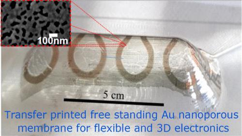
Large Area Freestanding Au Nanoporous Ultrathin Films Transfer Printed on Bendable Substrates and 3D Surfaces for Flexible Electronics
Conductive films based on metal nanomaterials have been studied as electrical interconnects for flexible electronics. Among them, freestanding ultrathin films are flexible, making them ideal candidates for integration onto 3D surfaces with complex shapes. Nevertheless, obtaining self-supported films of a few tens of nm with an area of several cm2 without breaking them is difficult. The solution proposed in this work is to get the films floating on the water surface before transferring them to 3D flexible surfaces by a water transfer printing process. Herein, we report the fabrication of stable and homogeneous Au nanoporous films with a thickness range of 6–60 nm and a floating surface area of several tens of cm2 on the water surface. The process combines Au and Cu magnetron sputtering deposition, Cu dealloying, and etching in acid vapor. We show that the transfer of such ultrathin films with a large area from the water surface onto the surface of flat flexible substrates or 3D surfaces is possible, maintaining conformability without significant electrical conductivity degradation. The thinnest films have a sheet resistance of about 10 Ω/□ with a transparency of about 50% at 550 nm. Because of their specific nanostructuration consisting of nanopores and interconnected nanoligaments, these films transferred to flexible flat surfaces can withstand bending for at least 3000 cycles with a curvature radius of 1 mm. Moreover, we show that a transfer of a design to a complex curved surface of 3D objects is possible using a 6 nm layer, whose role is to keep the geometry of the design during the transfer process.
期刊介绍:
ACS Applied Electronic Materials is an interdisciplinary journal publishing original research covering all aspects of electronic materials. The journal is devoted to reports of new and original experimental and theoretical research of an applied nature that integrate knowledge in the areas of materials science, engineering, optics, physics, and chemistry into important applications of electronic materials. Sample research topics that span the journal's scope are inorganic, organic, ionic and polymeric materials with properties that include conducting, semiconducting, superconducting, insulating, dielectric, magnetic, optoelectronic, piezoelectric, ferroelectric and thermoelectric.
Indexed/Abstracted:
Web of Science SCIE
Scopus
CAS
INSPEC
Portico


 求助内容:
求助内容: 应助结果提醒方式:


