Hung-I. Lin, Jeffrey Geldmeier, Erwan Baleine, Fan Yang, Sensong An, Ying Pan, Clara Rivero-Baleine*, Tian Gu* and Juejun Hu,
{"title":"宽视场大面积长波红外硅金属透镜","authors":"Hung-I. Lin, Jeffrey Geldmeier, Erwan Baleine, Fan Yang, Sensong An, Ying Pan, Clara Rivero-Baleine*, Tian Gu* and Juejun Hu, ","doi":"10.1021/acsphotonics.4c00013","DOIUrl":null,"url":null,"abstract":"<p >Long-wave infrared (LWIR, 8–12 μm wavelengths) spectral spectra are of vital importance to thermal imaging. Conventional LWIR optics made from single-crystalline Ge and chalcogenide glasses are bulky and fragile. The challenge is exacerbated for wide-field-of-view (FOV) optics, which traditionally mandates multiple cascaded elements that severely add to complexity and cost. Here, we designed and experimentally realized a LWIR metalens platform based on bulk Si wafers featuring 140° FOV. The metalenses, which have diameters exceeding 4 cm, were fabricated using a scalable wafer-level process involving photolithography and deep reactive ion etching. Using a metalens-integrated focal plane array, we further demonstrated wide-angle thermal imaging.</p>","PeriodicalId":23,"journal":{"name":"ACS Photonics","volume":"11 5","pages":"1943–1949"},"PeriodicalIF":6.7000,"publicationDate":"2024-04-09","publicationTypes":"Journal Article","fieldsOfStudy":null,"isOpenAccess":false,"openAccessPdf":"","citationCount":"0","resultStr":"{\"title\":\"Wide-Field-of-View, Large-Area Long-Wave Infrared Silicon Metalenses\",\"authors\":\"Hung-I. Lin, Jeffrey Geldmeier, Erwan Baleine, Fan Yang, Sensong An, Ying Pan, Clara Rivero-Baleine*, Tian Gu* and Juejun Hu, \",\"doi\":\"10.1021/acsphotonics.4c00013\",\"DOIUrl\":null,\"url\":null,\"abstract\":\"<p >Long-wave infrared (LWIR, 8–12 μm wavelengths) spectral spectra are of vital importance to thermal imaging. Conventional LWIR optics made from single-crystalline Ge and chalcogenide glasses are bulky and fragile. The challenge is exacerbated for wide-field-of-view (FOV) optics, which traditionally mandates multiple cascaded elements that severely add to complexity and cost. Here, we designed and experimentally realized a LWIR metalens platform based on bulk Si wafers featuring 140° FOV. The metalenses, which have diameters exceeding 4 cm, were fabricated using a scalable wafer-level process involving photolithography and deep reactive ion etching. Using a metalens-integrated focal plane array, we further demonstrated wide-angle thermal imaging.</p>\",\"PeriodicalId\":23,\"journal\":{\"name\":\"ACS Photonics\",\"volume\":\"11 5\",\"pages\":\"1943–1949\"},\"PeriodicalIF\":6.7000,\"publicationDate\":\"2024-04-09\",\"publicationTypes\":\"Journal Article\",\"fieldsOfStudy\":null,\"isOpenAccess\":false,\"openAccessPdf\":\"\",\"citationCount\":\"0\",\"resultStr\":null,\"platform\":\"Semanticscholar\",\"paperid\":null,\"PeriodicalName\":\"ACS Photonics\",\"FirstCategoryId\":\"101\",\"ListUrlMain\":\"https://pubs.acs.org/doi/10.1021/acsphotonics.4c00013\",\"RegionNum\":1,\"RegionCategory\":\"物理与天体物理\",\"ArticlePicture\":[],\"TitleCN\":null,\"AbstractTextCN\":null,\"PMCID\":null,\"EPubDate\":\"\",\"PubModel\":\"\",\"JCR\":\"Q1\",\"JCRName\":\"MATERIALS SCIENCE, MULTIDISCIPLINARY\",\"Score\":null,\"Total\":0}","platform":"Semanticscholar","paperid":null,"PeriodicalName":"ACS Photonics","FirstCategoryId":"101","ListUrlMain":"https://pubs.acs.org/doi/10.1021/acsphotonics.4c00013","RegionNum":1,"RegionCategory":"物理与天体物理","ArticlePicture":[],"TitleCN":null,"AbstractTextCN":null,"PMCID":null,"EPubDate":"","PubModel":"","JCR":"Q1","JCRName":"MATERIALS SCIENCE, MULTIDISCIPLINARY","Score":null,"Total":0}
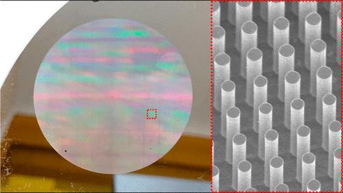
Long-wave infrared (LWIR, 8–12 μm wavelengths) spectral spectra are of vital importance to thermal imaging. Conventional LWIR optics made from single-crystalline Ge and chalcogenide glasses are bulky and fragile. The challenge is exacerbated for wide-field-of-view (FOV) optics, which traditionally mandates multiple cascaded elements that severely add to complexity and cost. Here, we designed and experimentally realized a LWIR metalens platform based on bulk Si wafers featuring 140° FOV. The metalenses, which have diameters exceeding 4 cm, were fabricated using a scalable wafer-level process involving photolithography and deep reactive ion etching. Using a metalens-integrated focal plane array, we further demonstrated wide-angle thermal imaging.
期刊介绍:
Published as soon as accepted and summarized in monthly issues, ACS Photonics will publish Research Articles, Letters, Perspectives, and Reviews, to encompass the full scope of published research in this field.


 求助内容:
求助内容: 应助结果提醒方式:


