Chi Zhang , Guoxian Zeng , Pengrong Lin , Hengtong Guo , ShiMeng Xu , XiaoChen Xie , Fuliang Wang
{"title":"利用旋转阴极实现高纵横比 TSV 填充的 12 英寸晶圆均匀性研究","authors":"Chi Zhang , Guoxian Zeng , Pengrong Lin , Hengtong Guo , ShiMeng Xu , XiaoChen Xie , Fuliang Wang","doi":"10.1016/j.mee.2024.112181","DOIUrl":null,"url":null,"abstract":"<div><p>In 2.5/3D(2.5/3-dimensional) packages, TSV (Through-Silicon Via) technology is crucial for achieving high performance and low power consumption. However, there are still challenges when it comes to uniformly filling TSVs on 300 mm whole wafers without defects. This study focuses on addressing this issue by designing a rotating cathode carrier with a 300 mm diameter, simulating the plating environment in different areas of a 300 mm wafer. The effects of plating conditions, such as cathode rotational speed and chip mounting position, on the filling of TSV are investigated. The TSV have a hole diameter of 10 μm and a depth of 100 μm.The findings reveal that when the cathode carrier rotates at a speed of 30 rpm, different areas of the analog wafer exhibit complete filling of TSV. Additionally, a surface plating layer with an average thickness of approximately 3 μm is obtained.</p></div>","PeriodicalId":18557,"journal":{"name":"Microelectronic Engineering","volume":"292 ","pages":"Article 112181"},"PeriodicalIF":2.6000,"publicationDate":"2024-03-20","publicationTypes":"Journal Article","fieldsOfStudy":null,"isOpenAccess":false,"openAccessPdf":"","citationCount":"0","resultStr":"{\"title\":\"Study on the 12 in. wafer uniformity of high aspect ratio TSV filling by using rotation cathode\",\"authors\":\"Chi Zhang , Guoxian Zeng , Pengrong Lin , Hengtong Guo , ShiMeng Xu , XiaoChen Xie , Fuliang Wang\",\"doi\":\"10.1016/j.mee.2024.112181\",\"DOIUrl\":null,\"url\":null,\"abstract\":\"<div><p>In 2.5/3D(2.5/3-dimensional) packages, TSV (Through-Silicon Via) technology is crucial for achieving high performance and low power consumption. However, there are still challenges when it comes to uniformly filling TSVs on 300 mm whole wafers without defects. This study focuses on addressing this issue by designing a rotating cathode carrier with a 300 mm diameter, simulating the plating environment in different areas of a 300 mm wafer. The effects of plating conditions, such as cathode rotational speed and chip mounting position, on the filling of TSV are investigated. The TSV have a hole diameter of 10 μm and a depth of 100 μm.The findings reveal that when the cathode carrier rotates at a speed of 30 rpm, different areas of the analog wafer exhibit complete filling of TSV. Additionally, a surface plating layer with an average thickness of approximately 3 μm is obtained.</p></div>\",\"PeriodicalId\":18557,\"journal\":{\"name\":\"Microelectronic Engineering\",\"volume\":\"292 \",\"pages\":\"Article 112181\"},\"PeriodicalIF\":2.6000,\"publicationDate\":\"2024-03-20\",\"publicationTypes\":\"Journal Article\",\"fieldsOfStudy\":null,\"isOpenAccess\":false,\"openAccessPdf\":\"\",\"citationCount\":\"0\",\"resultStr\":null,\"platform\":\"Semanticscholar\",\"paperid\":null,\"PeriodicalName\":\"Microelectronic Engineering\",\"FirstCategoryId\":\"5\",\"ListUrlMain\":\"https://www.sciencedirect.com/science/article/pii/S0167931724000509\",\"RegionNum\":4,\"RegionCategory\":\"工程技术\",\"ArticlePicture\":[],\"TitleCN\":null,\"AbstractTextCN\":null,\"PMCID\":null,\"EPubDate\":\"\",\"PubModel\":\"\",\"JCR\":\"Q2\",\"JCRName\":\"ENGINEERING, ELECTRICAL & ELECTRONIC\",\"Score\":null,\"Total\":0}","platform":"Semanticscholar","paperid":null,"PeriodicalName":"Microelectronic Engineering","FirstCategoryId":"5","ListUrlMain":"https://www.sciencedirect.com/science/article/pii/S0167931724000509","RegionNum":4,"RegionCategory":"工程技术","ArticlePicture":[],"TitleCN":null,"AbstractTextCN":null,"PMCID":null,"EPubDate":"","PubModel":"","JCR":"Q2","JCRName":"ENGINEERING, ELECTRICAL & ELECTRONIC","Score":null,"Total":0}
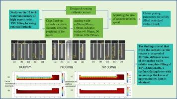
Study on the 12 in. wafer uniformity of high aspect ratio TSV filling by using rotation cathode
In 2.5/3D(2.5/3-dimensional) packages, TSV (Through-Silicon Via) technology is crucial for achieving high performance and low power consumption. However, there are still challenges when it comes to uniformly filling TSVs on 300 mm whole wafers without defects. This study focuses on addressing this issue by designing a rotating cathode carrier with a 300 mm diameter, simulating the plating environment in different areas of a 300 mm wafer. The effects of plating conditions, such as cathode rotational speed and chip mounting position, on the filling of TSV are investigated. The TSV have a hole diameter of 10 μm and a depth of 100 μm.The findings reveal that when the cathode carrier rotates at a speed of 30 rpm, different areas of the analog wafer exhibit complete filling of TSV. Additionally, a surface plating layer with an average thickness of approximately 3 μm is obtained.
期刊介绍:
Microelectronic Engineering is the premier nanoprocessing, and nanotechnology journal focusing on fabrication of electronic, photonic, bioelectronic, electromechanic and fluidic devices and systems, and their applications in the broad areas of electronics, photonics, energy, life sciences, and environment. It covers also the expanding interdisciplinary field of "more than Moore" and "beyond Moore" integrated nanoelectronics / photonics and micro-/nano-/bio-systems. Through its unique mixture of peer-reviewed articles, reviews, accelerated publications, short and Technical notes, and the latest research news on key developments, Microelectronic Engineering provides comprehensive coverage of this exciting, interdisciplinary and dynamic new field for researchers in academia and professionals in industry.

 求助内容:
求助内容: 应助结果提醒方式:


