Yu. Yu. Illarionov, T. Knobloch, B. Uzlu, A. G. Banshchikov, I. A. Ivanov, V. Sverdlov, M. Otto, S. L. Stoll, M. I. Vexler, M. Waltl, Z. Wang, B. Manna, D. Neumaier, M. C. Lemme, N. S. Sokolov, T. Grasser
{"title":"具有薄外延 CaF2 绝缘层的石墨烯场效应晶体管的变异性和高温可靠性","authors":"Yu. Yu. Illarionov, T. Knobloch, B. Uzlu, A. G. Banshchikov, I. A. Ivanov, V. Sverdlov, M. Otto, S. L. Stoll, M. I. Vexler, M. Waltl, Z. Wang, B. Manna, D. Neumaier, M. C. Lemme, N. S. Sokolov, T. Grasser","doi":"10.1038/s41699-024-00461-0","DOIUrl":null,"url":null,"abstract":"Graphene is a promising material for applications as a channel in graphene field-effect transistors (GFETs) which may be used as a building block for optoelectronics, high-frequency devices and sensors. However, these devices require gate insulators which ideally should form atomically flat interfaces with graphene and at the same time contain small densities of traps to maintain high device stability. Previously used amorphous oxides, such as SiO2 and Al2O3, however, typically suffer from oxide dangling bonds at the interface, high surface roughness and numerous border oxide traps. In order to address these challenges, here we use 2 nm thick epitaxial CaF2 as a gate insulator in GFETs. By analyzing device-to-device variability for about 200 devices fabricated in two batches, we find that tens of them show similar gate transfer characteristics. Our statistical analysis of the hysteresis up to 175oC has revealed that while an ambient-sensitive counterclockwise hysteresis can be present in some devices, the dominant mechanism is thermally activated charge trapping by border defects in CaF2 which results in the conventional clockwise hysteresis. We demonstrate that both the hysteresis and bias-temperature instabilities in our GFETs with CaF2 are comparable to similar devices with SiO2 and Al2O3. In particular, we achieve a small hysteresis below 0.01 V for equivalent oxide thickness (EOT) of about 1 nm at the electric fields up to 15 MV cm−1 and sweep times in the kilosecond range. Thus, our results demonstrate that crystalline CaF2 is a promising insulator for highly-stable GFETs.","PeriodicalId":19227,"journal":{"name":"npj 2D Materials and Applications","volume":" ","pages":"1-10"},"PeriodicalIF":9.1000,"publicationDate":"2024-03-19","publicationTypes":"Journal Article","fieldsOfStudy":null,"isOpenAccess":false,"openAccessPdf":"https://www.nature.com/articles/s41699-024-00461-0.pdf","citationCount":"0","resultStr":"{\"title\":\"Variability and high temperature reliability of graphene field-effect transistors with thin epitaxial CaF2 insulators\",\"authors\":\"Yu. Yu. Illarionov, T. Knobloch, B. Uzlu, A. G. Banshchikov, I. A. Ivanov, V. Sverdlov, M. Otto, S. L. Stoll, M. I. Vexler, M. Waltl, Z. Wang, B. Manna, D. Neumaier, M. C. Lemme, N. S. Sokolov, T. Grasser\",\"doi\":\"10.1038/s41699-024-00461-0\",\"DOIUrl\":null,\"url\":null,\"abstract\":\"Graphene is a promising material for applications as a channel in graphene field-effect transistors (GFETs) which may be used as a building block for optoelectronics, high-frequency devices and sensors. However, these devices require gate insulators which ideally should form atomically flat interfaces with graphene and at the same time contain small densities of traps to maintain high device stability. Previously used amorphous oxides, such as SiO2 and Al2O3, however, typically suffer from oxide dangling bonds at the interface, high surface roughness and numerous border oxide traps. In order to address these challenges, here we use 2 nm thick epitaxial CaF2 as a gate insulator in GFETs. By analyzing device-to-device variability for about 200 devices fabricated in two batches, we find that tens of them show similar gate transfer characteristics. Our statistical analysis of the hysteresis up to 175oC has revealed that while an ambient-sensitive counterclockwise hysteresis can be present in some devices, the dominant mechanism is thermally activated charge trapping by border defects in CaF2 which results in the conventional clockwise hysteresis. We demonstrate that both the hysteresis and bias-temperature instabilities in our GFETs with CaF2 are comparable to similar devices with SiO2 and Al2O3. In particular, we achieve a small hysteresis below 0.01 V for equivalent oxide thickness (EOT) of about 1 nm at the electric fields up to 15 MV cm−1 and sweep times in the kilosecond range. Thus, our results demonstrate that crystalline CaF2 is a promising insulator for highly-stable GFETs.\",\"PeriodicalId\":19227,\"journal\":{\"name\":\"npj 2D Materials and Applications\",\"volume\":\" \",\"pages\":\"1-10\"},\"PeriodicalIF\":9.1000,\"publicationDate\":\"2024-03-19\",\"publicationTypes\":\"Journal Article\",\"fieldsOfStudy\":null,\"isOpenAccess\":false,\"openAccessPdf\":\"https://www.nature.com/articles/s41699-024-00461-0.pdf\",\"citationCount\":\"0\",\"resultStr\":null,\"platform\":\"Semanticscholar\",\"paperid\":null,\"PeriodicalName\":\"npj 2D Materials and Applications\",\"FirstCategoryId\":\"88\",\"ListUrlMain\":\"https://www.nature.com/articles/s41699-024-00461-0\",\"RegionNum\":2,\"RegionCategory\":\"材料科学\",\"ArticlePicture\":[],\"TitleCN\":null,\"AbstractTextCN\":null,\"PMCID\":null,\"EPubDate\":\"\",\"PubModel\":\"\",\"JCR\":\"Q1\",\"JCRName\":\"MATERIALS SCIENCE, MULTIDISCIPLINARY\",\"Score\":null,\"Total\":0}","platform":"Semanticscholar","paperid":null,"PeriodicalName":"npj 2D Materials and Applications","FirstCategoryId":"88","ListUrlMain":"https://www.nature.com/articles/s41699-024-00461-0","RegionNum":2,"RegionCategory":"材料科学","ArticlePicture":[],"TitleCN":null,"AbstractTextCN":null,"PMCID":null,"EPubDate":"","PubModel":"","JCR":"Q1","JCRName":"MATERIALS SCIENCE, MULTIDISCIPLINARY","Score":null,"Total":0}
Variability and high temperature reliability of graphene field-effect transistors with thin epitaxial CaF2 insulators
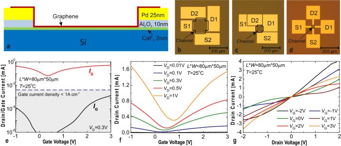
Graphene is a promising material for applications as a channel in graphene field-effect transistors (GFETs) which may be used as a building block for optoelectronics, high-frequency devices and sensors. However, these devices require gate insulators which ideally should form atomically flat interfaces with graphene and at the same time contain small densities of traps to maintain high device stability. Previously used amorphous oxides, such as SiO2 and Al2O3, however, typically suffer from oxide dangling bonds at the interface, high surface roughness and numerous border oxide traps. In order to address these challenges, here we use 2 nm thick epitaxial CaF2 as a gate insulator in GFETs. By analyzing device-to-device variability for about 200 devices fabricated in two batches, we find that tens of them show similar gate transfer characteristics. Our statistical analysis of the hysteresis up to 175oC has revealed that while an ambient-sensitive counterclockwise hysteresis can be present in some devices, the dominant mechanism is thermally activated charge trapping by border defects in CaF2 which results in the conventional clockwise hysteresis. We demonstrate that both the hysteresis and bias-temperature instabilities in our GFETs with CaF2 are comparable to similar devices with SiO2 and Al2O3. In particular, we achieve a small hysteresis below 0.01 V for equivalent oxide thickness (EOT) of about 1 nm at the electric fields up to 15 MV cm−1 and sweep times in the kilosecond range. Thus, our results demonstrate that crystalline CaF2 is a promising insulator for highly-stable GFETs.
期刊介绍:
npj 2D Materials and Applications publishes papers on the fundamental behavior, synthesis, properties and applications of existing and emerging 2D materials. By selecting papers with the potential for impact, the journal aims to facilitate the transfer of the research of 2D materials into wide-ranging applications.