{"title":"使用 gm/ID 方法的 AB 类运算放大器设计方法","authors":"Chen Chen, Jinxing Cheng, Hongyi Wang, Youyou Fan, Kaikai Wu, Tao Tao, Qingbo Wang, Ai Yu, Weiwei Wen, Youpeng Wu, Yue Zhang","doi":"10.1007/s10470-024-02252-5","DOIUrl":null,"url":null,"abstract":"<div><p>The primary contribution of this paper is the extension of the g<sub>m</sub>/I<sub>D</sub> design methodology to two-stage operational amplifiers with class-AB output stages. First, the circuit is analyzed from the perspective of the g<sub>m</sub>/I<sub>D</sub> methodology, with a focus on its performance metrics and constraints. Second, to handle optimization targets and constraints automatically, the circuit sizing task is formulated as a single-objective optimization problem, and an optimizer is employed to obtain the temporary solution automatically. Benefiting from the g<sub>m</sub>/I<sub>D</sub> methodology, the gap between analytical equations and circuit simulation is highly reduced. Third, following the temporary solution, a guided fine-tuning method is introduced to further optimize the temporary solution. To demonstrate the effectiveness of this approach, we compared the equation-based method using the square-law model, two simulation-based methods and a commercial tool, Cadence ADE GXL, employing SMIC 55 nm and SMIC 180 nm CMOS technologies. The simulation results confirm the success of the proposed approach, showing that it not only reduces the gap between analytical equations and simulations, but also achieves the best performance metrics.</p></div>","PeriodicalId":7827,"journal":{"name":"Analog Integrated Circuits and Signal Processing","volume":"119 1","pages":"43 - 55"},"PeriodicalIF":1.2000,"publicationDate":"2024-02-11","publicationTypes":"Journal Article","fieldsOfStudy":null,"isOpenAccess":false,"openAccessPdf":"","citationCount":"0","resultStr":"{\"title\":\"A design approach for class-AB operational amplifier using the gm/ID methodology\",\"authors\":\"Chen Chen, Jinxing Cheng, Hongyi Wang, Youyou Fan, Kaikai Wu, Tao Tao, Qingbo Wang, Ai Yu, Weiwei Wen, Youpeng Wu, Yue Zhang\",\"doi\":\"10.1007/s10470-024-02252-5\",\"DOIUrl\":null,\"url\":null,\"abstract\":\"<div><p>The primary contribution of this paper is the extension of the g<sub>m</sub>/I<sub>D</sub> design methodology to two-stage operational amplifiers with class-AB output stages. First, the circuit is analyzed from the perspective of the g<sub>m</sub>/I<sub>D</sub> methodology, with a focus on its performance metrics and constraints. Second, to handle optimization targets and constraints automatically, the circuit sizing task is formulated as a single-objective optimization problem, and an optimizer is employed to obtain the temporary solution automatically. Benefiting from the g<sub>m</sub>/I<sub>D</sub> methodology, the gap between analytical equations and circuit simulation is highly reduced. Third, following the temporary solution, a guided fine-tuning method is introduced to further optimize the temporary solution. To demonstrate the effectiveness of this approach, we compared the equation-based method using the square-law model, two simulation-based methods and a commercial tool, Cadence ADE GXL, employing SMIC 55 nm and SMIC 180 nm CMOS technologies. The simulation results confirm the success of the proposed approach, showing that it not only reduces the gap between analytical equations and simulations, but also achieves the best performance metrics.</p></div>\",\"PeriodicalId\":7827,\"journal\":{\"name\":\"Analog Integrated Circuits and Signal Processing\",\"volume\":\"119 1\",\"pages\":\"43 - 55\"},\"PeriodicalIF\":1.2000,\"publicationDate\":\"2024-02-11\",\"publicationTypes\":\"Journal Article\",\"fieldsOfStudy\":null,\"isOpenAccess\":false,\"openAccessPdf\":\"\",\"citationCount\":\"0\",\"resultStr\":null,\"platform\":\"Semanticscholar\",\"paperid\":null,\"PeriodicalName\":\"Analog Integrated Circuits and Signal Processing\",\"FirstCategoryId\":\"5\",\"ListUrlMain\":\"https://link.springer.com/article/10.1007/s10470-024-02252-5\",\"RegionNum\":4,\"RegionCategory\":\"工程技术\",\"ArticlePicture\":[],\"TitleCN\":null,\"AbstractTextCN\":null,\"PMCID\":null,\"EPubDate\":\"\",\"PubModel\":\"\",\"JCR\":\"Q4\",\"JCRName\":\"COMPUTER SCIENCE, HARDWARE & ARCHITECTURE\",\"Score\":null,\"Total\":0}","platform":"Semanticscholar","paperid":null,"PeriodicalName":"Analog Integrated Circuits and Signal Processing","FirstCategoryId":"5","ListUrlMain":"https://link.springer.com/article/10.1007/s10470-024-02252-5","RegionNum":4,"RegionCategory":"工程技术","ArticlePicture":[],"TitleCN":null,"AbstractTextCN":null,"PMCID":null,"EPubDate":"","PubModel":"","JCR":"Q4","JCRName":"COMPUTER SCIENCE, HARDWARE & ARCHITECTURE","Score":null,"Total":0}
A design approach for class-AB operational amplifier using the gm/ID methodology
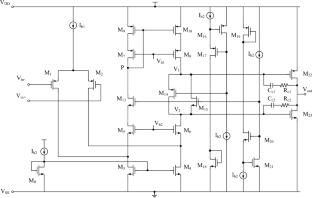
The primary contribution of this paper is the extension of the gm/ID design methodology to two-stage operational amplifiers with class-AB output stages. First, the circuit is analyzed from the perspective of the gm/ID methodology, with a focus on its performance metrics and constraints. Second, to handle optimization targets and constraints automatically, the circuit sizing task is formulated as a single-objective optimization problem, and an optimizer is employed to obtain the temporary solution automatically. Benefiting from the gm/ID methodology, the gap between analytical equations and circuit simulation is highly reduced. Third, following the temporary solution, a guided fine-tuning method is introduced to further optimize the temporary solution. To demonstrate the effectiveness of this approach, we compared the equation-based method using the square-law model, two simulation-based methods and a commercial tool, Cadence ADE GXL, employing SMIC 55 nm and SMIC 180 nm CMOS technologies. The simulation results confirm the success of the proposed approach, showing that it not only reduces the gap between analytical equations and simulations, but also achieves the best performance metrics.
期刊介绍:
Analog Integrated Circuits and Signal Processing is an archival peer reviewed journal dedicated to the design and application of analog, radio frequency (RF), and mixed signal integrated circuits (ICs) as well as signal processing circuits and systems. It features both new research results and tutorial views and reflects the large volume of cutting-edge research activity in the worldwide field today.
A partial list of topics includes analog and mixed signal interface circuits and systems; analog and RFIC design; data converters; active-RC, switched-capacitor, and continuous-time integrated filters; mixed analog/digital VLSI systems; wireless radio transceivers; clock and data recovery circuits; and high speed optoelectronic circuits and systems.


 求助内容:
求助内容: 应助结果提醒方式:


