Santhanu Panikar Ramanandan, Joel Reñé Sapera, Alban Morelle, Sara Martí-Sánchez, Alok Rudra, Jordi Arbiol, Vladimir G. Dubrovskii and Anna Fontcuberta i Morral
{"title":"控制 Ge 岛凝聚以在硅上形成纳米线。","authors":"Santhanu Panikar Ramanandan, Joel Reñé Sapera, Alban Morelle, Sara Martí-Sánchez, Alok Rudra, Jordi Arbiol, Vladimir G. Dubrovskii and Anna Fontcuberta i Morral","doi":"10.1039/D3NH00573A","DOIUrl":null,"url":null,"abstract":"<p >Germanium nanowires could be the building blocks of hole-spin qubit quantum computers. Selective area epitaxy enables the direct integration of Ge nanowires on a silicon chip while controlling the device design, density, and scalability. For this to become a reality, it is essential to understand and control the initial stages of the epitaxy process. In this work, we highlight the importance of surface treatment in the reactor prior to growth to achieve high crystal quality and connected Ge nanowire structures. In particular, we demonstrate that exposure to AsH<small><sub>3</sub></small> during the high-temperature treatment enhances lateral growth of initial Ge islands and promotes faster formation of continuous Ge nanowires in trenches. The Kolmogorov–Johnson–Mehl–Avrami crystallization model supports our explanation of Ge coalescence. These results provide critical insight into the selective epitaxy of horizontal Ge nanowires on lattice-mismatched Si substrates, which can be translated to other material systems.</p>","PeriodicalId":93,"journal":{"name":"Nanoscale Horizons","volume":" 4","pages":" 555-565"},"PeriodicalIF":6.6000,"publicationDate":"2024-02-12","publicationTypes":"Journal Article","fieldsOfStudy":null,"isOpenAccess":false,"openAccessPdf":"https://pubs.rsc.org/en/content/articlepdf/2024/nh/d3nh00573a?page=search","citationCount":"0","resultStr":"{\"title\":\"Control of Ge island coalescence for the formation of nanowires on silicon†\",\"authors\":\"Santhanu Panikar Ramanandan, Joel Reñé Sapera, Alban Morelle, Sara Martí-Sánchez, Alok Rudra, Jordi Arbiol, Vladimir G. Dubrovskii and Anna Fontcuberta i Morral\",\"doi\":\"10.1039/D3NH00573A\",\"DOIUrl\":null,\"url\":null,\"abstract\":\"<p >Germanium nanowires could be the building blocks of hole-spin qubit quantum computers. Selective area epitaxy enables the direct integration of Ge nanowires on a silicon chip while controlling the device design, density, and scalability. For this to become a reality, it is essential to understand and control the initial stages of the epitaxy process. In this work, we highlight the importance of surface treatment in the reactor prior to growth to achieve high crystal quality and connected Ge nanowire structures. In particular, we demonstrate that exposure to AsH<small><sub>3</sub></small> during the high-temperature treatment enhances lateral growth of initial Ge islands and promotes faster formation of continuous Ge nanowires in trenches. The Kolmogorov–Johnson–Mehl–Avrami crystallization model supports our explanation of Ge coalescence. These results provide critical insight into the selective epitaxy of horizontal Ge nanowires on lattice-mismatched Si substrates, which can be translated to other material systems.</p>\",\"PeriodicalId\":93,\"journal\":{\"name\":\"Nanoscale Horizons\",\"volume\":\" 4\",\"pages\":\" 555-565\"},\"PeriodicalIF\":6.6000,\"publicationDate\":\"2024-02-12\",\"publicationTypes\":\"Journal Article\",\"fieldsOfStudy\":null,\"isOpenAccess\":false,\"openAccessPdf\":\"https://pubs.rsc.org/en/content/articlepdf/2024/nh/d3nh00573a?page=search\",\"citationCount\":\"0\",\"resultStr\":null,\"platform\":\"Semanticscholar\",\"paperid\":null,\"PeriodicalName\":\"Nanoscale Horizons\",\"FirstCategoryId\":\"88\",\"ListUrlMain\":\"https://pubs.rsc.org/en/content/articlelanding/2024/nh/d3nh00573a\",\"RegionNum\":2,\"RegionCategory\":\"材料科学\",\"ArticlePicture\":[],\"TitleCN\":null,\"AbstractTextCN\":null,\"PMCID\":null,\"EPubDate\":\"\",\"PubModel\":\"\",\"JCR\":\"Q1\",\"JCRName\":\"CHEMISTRY, PHYSICAL\",\"Score\":null,\"Total\":0}","platform":"Semanticscholar","paperid":null,"PeriodicalName":"Nanoscale Horizons","FirstCategoryId":"88","ListUrlMain":"https://pubs.rsc.org/en/content/articlelanding/2024/nh/d3nh00573a","RegionNum":2,"RegionCategory":"材料科学","ArticlePicture":[],"TitleCN":null,"AbstractTextCN":null,"PMCID":null,"EPubDate":"","PubModel":"","JCR":"Q1","JCRName":"CHEMISTRY, PHYSICAL","Score":null,"Total":0}
引用次数: 0
摘要
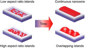
锗纳米线可以成为空穴-自旋量子比特量子计算机的构件。通过选择性区域外延,可以在硅芯片上直接集成锗纳米线,同时控制器件的设计、密度和可扩展性。要实现这一目标,了解和控制外延过程的初始阶段至关重要。在这项工作中,我们强调了生长前在反应器中进行表面处理对获得高晶体质量和连接的 Ge 纳米线结构的重要性。特别是,我们证明了在高温处理过程中暴露于 AsH3 会增强初始 Ge 岛的横向生长,并促进沟槽中连续 Ge 纳米线的快速形成。Kolmogorov-Johnson-Mehl-Avrami 结晶模型支持我们对 Ge 凝聚的解释。这些结果为在晶格不匹配的硅衬底上选择性外延水平 Ge 纳米线提供了重要的启示,可应用于其他材料体系。
Control of Ge island coalescence for the formation of nanowires on silicon†
Germanium nanowires could be the building blocks of hole-spin qubit quantum computers. Selective area epitaxy enables the direct integration of Ge nanowires on a silicon chip while controlling the device design, density, and scalability. For this to become a reality, it is essential to understand and control the initial stages of the epitaxy process. In this work, we highlight the importance of surface treatment in the reactor prior to growth to achieve high crystal quality and connected Ge nanowire structures. In particular, we demonstrate that exposure to AsH3 during the high-temperature treatment enhances lateral growth of initial Ge islands and promotes faster formation of continuous Ge nanowires in trenches. The Kolmogorov–Johnson–Mehl–Avrami crystallization model supports our explanation of Ge coalescence. These results provide critical insight into the selective epitaxy of horizontal Ge nanowires on lattice-mismatched Si substrates, which can be translated to other material systems.
期刊介绍:
Nanoscale Horizons stands out as a premier journal for publishing exceptionally high-quality and innovative nanoscience and nanotechnology. The emphasis lies on original research that introduces a new concept or a novel perspective (a conceptual advance), prioritizing this over reporting technological improvements. Nevertheless, outstanding articles showcasing truly groundbreaking developments, including record-breaking performance, may also find a place in the journal. Published work must be of substantial general interest to our broad and diverse readership across the nanoscience and nanotechnology community.

 求助内容:
求助内容: 应助结果提醒方式:


