工艺对 300 mm FAB MoS2 场效应晶体管稳定性和可靠性的影响

IF 9.1 2区 材料科学 Q1 MATERIALS SCIENCE, MULTIDISCIPLINARY
Yu. Yu. Illarionov, A. Karl, Q. Smets, B. Kaczer, T. Knobloch, L. Panarella, T. Schram, S. Brems, D. Cott, I. Asselberghs, T. Grasser
{"title":"工艺对 300 mm FAB MoS2 场效应晶体管稳定性和可靠性的影响","authors":"Yu. Yu. Illarionov, A. Karl, Q. Smets, B. Kaczer, T. Knobloch, L. Panarella, T. Schram, S. Brems, D. Cott, I. Asselberghs, T. Grasser","doi":"10.1038/s41699-024-00445-0","DOIUrl":null,"url":null,"abstract":"Recent advances in fabricating field-effect transistors with MoS2 and other related two-dimensional (2D) semiconductors have inspired the industry to begin with the integration of these emerging technologies into FAB-compatible process flows. Just like in the lab research on 2D devices performed in the last decade, focus during development is typically put on pure technology-related issues, such as low-temperature growth methods of large-area 2D films on target substrates, damage-free transfer from sacrificial substrates and growth of top-gate oxides. With maturing technology, the problem of stability limitations caused by oxide traps is gradually coming into focus now. Thus, here we report an in-depth analysis of hysteresis and bias-temperature instabilities for MoS2 FETs fabricated using a 300 mm FAB-compatible process. By performing a comprehensive statistical analysis on devices with top gate lengths ranging between 18 nm and 10 μm, we demonstrate that aggressive scaling results in additional stability problems, likely caused by defective edges of the scaled top gates, in particular at higher operation temperatures. These are important insights for understanding and addressing the stability limitations in future nanoscale 2D FETs produced using FAB process lines.","PeriodicalId":19227,"journal":{"name":"npj 2D Materials and Applications","volume":" ","pages":"1-7"},"PeriodicalIF":9.1000,"publicationDate":"2024-02-02","publicationTypes":"Journal Article","fieldsOfStudy":null,"isOpenAccess":false,"openAccessPdf":"https://www.nature.com/articles/s41699-024-00445-0.pdf","citationCount":"0","resultStr":"{\"title\":\"Process implications on the stability and reliability of 300 mm FAB MoS2 field-effect transistors\",\"authors\":\"Yu. Yu. Illarionov, A. Karl, Q. Smets, B. Kaczer, T. Knobloch, L. Panarella, T. Schram, S. Brems, D. Cott, I. Asselberghs, T. Grasser\",\"doi\":\"10.1038/s41699-024-00445-0\",\"DOIUrl\":null,\"url\":null,\"abstract\":\"Recent advances in fabricating field-effect transistors with MoS2 and other related two-dimensional (2D) semiconductors have inspired the industry to begin with the integration of these emerging technologies into FAB-compatible process flows. Just like in the lab research on 2D devices performed in the last decade, focus during development is typically put on pure technology-related issues, such as low-temperature growth methods of large-area 2D films on target substrates, damage-free transfer from sacrificial substrates and growth of top-gate oxides. With maturing technology, the problem of stability limitations caused by oxide traps is gradually coming into focus now. Thus, here we report an in-depth analysis of hysteresis and bias-temperature instabilities for MoS2 FETs fabricated using a 300 mm FAB-compatible process. By performing a comprehensive statistical analysis on devices with top gate lengths ranging between 18 nm and 10 μm, we demonstrate that aggressive scaling results in additional stability problems, likely caused by defective edges of the scaled top gates, in particular at higher operation temperatures. These are important insights for understanding and addressing the stability limitations in future nanoscale 2D FETs produced using FAB process lines.\",\"PeriodicalId\":19227,\"journal\":{\"name\":\"npj 2D Materials and Applications\",\"volume\":\" \",\"pages\":\"1-7\"},\"PeriodicalIF\":9.1000,\"publicationDate\":\"2024-02-02\",\"publicationTypes\":\"Journal Article\",\"fieldsOfStudy\":null,\"isOpenAccess\":false,\"openAccessPdf\":\"https://www.nature.com/articles/s41699-024-00445-0.pdf\",\"citationCount\":\"0\",\"resultStr\":null,\"platform\":\"Semanticscholar\",\"paperid\":null,\"PeriodicalName\":\"npj 2D Materials and Applications\",\"FirstCategoryId\":\"88\",\"ListUrlMain\":\"https://www.nature.com/articles/s41699-024-00445-0\",\"RegionNum\":2,\"RegionCategory\":\"材料科学\",\"ArticlePicture\":[],\"TitleCN\":null,\"AbstractTextCN\":null,\"PMCID\":null,\"EPubDate\":\"\",\"PubModel\":\"\",\"JCR\":\"Q1\",\"JCRName\":\"MATERIALS SCIENCE, MULTIDISCIPLINARY\",\"Score\":null,\"Total\":0}","platform":"Semanticscholar","paperid":null,"PeriodicalName":"npj 2D Materials and Applications","FirstCategoryId":"88","ListUrlMain":"https://www.nature.com/articles/s41699-024-00445-0","RegionNum":2,"RegionCategory":"材料科学","ArticlePicture":[],"TitleCN":null,"AbstractTextCN":null,"PMCID":null,"EPubDate":"","PubModel":"","JCR":"Q1","JCRName":"MATERIALS SCIENCE, MULTIDISCIPLINARY","Score":null,"Total":0}
引用次数: 0

摘要

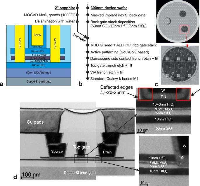
利用 MoS2 和其他相关二维(2D)半导体制造场效应晶体管方面的最新进展,促使业界开始将这些新兴技术集成到 FAB 兼容工艺流程中。与过去十年间进行的二维器件实验室研究一样,开发过程中的重点通常放在纯技术相关的问题上,如目标基底上大面积二维薄膜的低温生长方法、牺牲基底的无损转移以及顶栅氧化物的生长。随着技术的不断成熟,氧化物陷阱导致的稳定性限制问题也逐渐成为焦点。因此,我们在此报告了对使用 300 毫米 FAB 兼容工艺制造的 MoS2 FET 的磁滞和偏置-温度不稳定性的深入分析。通过对顶栅长度介于 18 nm 和 10 μm 之间的器件进行全面的统计分析,我们证明了激进的缩放会导致额外的稳定性问题,这可能是由缩放顶栅的缺陷边缘引起的,尤其是在较高的工作温度下。这些见解对于理解和解决未来使用 FAB 工艺线生产的纳米级二维场效应晶体管的稳定性限制问题非常重要。
本文章由计算机程序翻译,如有差异,请以英文原文为准。

Process implications on the stability and reliability of 300 mm FAB MoS2 field-effect transistors

Process implications on the stability and reliability of 300 mm FAB MoS2 field-effect transistors
Recent advances in fabricating field-effect transistors with MoS2 and other related two-dimensional (2D) semiconductors have inspired the industry to begin with the integration of these emerging technologies into FAB-compatible process flows. Just like in the lab research on 2D devices performed in the last decade, focus during development is typically put on pure technology-related issues, such as low-temperature growth methods of large-area 2D films on target substrates, damage-free transfer from sacrificial substrates and growth of top-gate oxides. With maturing technology, the problem of stability limitations caused by oxide traps is gradually coming into focus now. Thus, here we report an in-depth analysis of hysteresis and bias-temperature instabilities for MoS2 FETs fabricated using a 300 mm FAB-compatible process. By performing a comprehensive statistical analysis on devices with top gate lengths ranging between 18 nm and 10 μm, we demonstrate that aggressive scaling results in additional stability problems, likely caused by defective edges of the scaled top gates, in particular at higher operation temperatures. These are important insights for understanding and addressing the stability limitations in future nanoscale 2D FETs produced using FAB process lines.
求助全文
通过发布文献求助,成功后即可免费获取论文全文。 去求助
来源期刊

npj 2D Materials and Applications
npj 2D Materials and Applications Engineering-Mechanics of Materials
CiteScore
14.50
自引率
2.10%
发文量
80
审稿时长
15 weeks
期刊介绍: npj 2D Materials and Applications publishes papers on the fundamental behavior, synthesis, properties and applications of existing and emerging 2D materials. By selecting papers with the potential for impact, the journal aims to facilitate the transfer of the research of 2D materials into wide-ranging applications.
×
引用
GB/T 7714-2015
复制
MLA
复制
APA
复制
导出至
BibTeX EndNote RefMan NoteFirst NoteExpress
×
提示
您的信息不完整,为了账户安全,请先补充。
现在去补充
×
提示
您因"违规操作"
具体请查看互助需知
我知道了
×
提示
确定
请完成安全验证×
copy
已复制链接
快去分享给好友吧!
我知道了
右上角分享
点击右上角分享
0
联系我们:info@booksci.cn Book学术提供免费学术资源搜索服务,方便国内外学者检索中英文文献。致力于提供最便捷和优质的服务体验。 Copyright © 2023 布克学术 All rights reserved.
京ICP备2023020795号-1
ghs 京公网安备 11010802042870号
Book学术文献互助
Book学术文献互助群
群 号:481959085
Book学术官方微信