Saeed Naghavi, Kaisa Ryynänen, Mahwish Zahra, Aleksi Korsman, Kari Stadius, Marko Kosunen, Vishnu Unnikrishnan, Lauri Anttila, Mikko Valkama, Jussi Ryynänen
{"title":"用于 5G 应用的 18-28 GHz 双模下变频集成电路","authors":"Saeed Naghavi, Kaisa Ryynänen, Mahwish Zahra, Aleksi Korsman, Kari Stadius, Marko Kosunen, Vishnu Unnikrishnan, Lauri Anttila, Mikko Valkama, Jussi Ryynänen","doi":"10.1007/s10470-023-02232-1","DOIUrl":null,"url":null,"abstract":"<div><p>Emerging spectrum trends require a higher integration of 5G New Radio Frequency Range 1 (FR1) and Frequency Range 2 (FR2) bands to enhance the availability of spectrum and spectrum-sharing opportunities. To enable the reception of both FR1 and FR2 bands in a seamless hardware entity, we propose combining homodyne and heterodyne architectures. This necessitates the incorporation of a down-converter module that transfers the incoming signals from FR2 bands down to FR1, ensuring compatibility with an FR1 direct-conversion receiver (DCR) for the final signal reception. The primary focus of this paper is the design and implementation of the required integrated down-converter. The module includes an integrated balun, a low-noise amplifier (LNA) with a bypass mode, a dual-mode mixer, and an intermediate frequency (IF) amplifier. The introduced bypass mode helps to further elevate the linearity performance compared to the nominal mode. The bypass mode is designed for joint communication and sensing operation to avoid the compression of the receiver. This work also incorporates a local oscillator (LO) signal distribution network with phase tuning elements using a mixed-signal approach. The circuit is implemented in a 22-nm CMOS process, and the active die area is 0.6 <span>\\(\\text {mm}^\\text {2}\\)</span>. The measurements demonstrate that the implemented chip can efficiently perform the required frequency conversion over a wide frequency range of 18–28 GHz. Conversion gain of 4.5–7.5 dB, noise figure of 15–19.7 dB, 1 dB compression point (IP1dB) of − 16 to − 10 dBm, and input third-order intercept point (IIP3) of − 5 to 0 dBm are achieved. The measured IP1 dB and IIP3 for the bypass mode are +0.5 to +4.5 dBm and +8.5 to +10 dBm, respectively.</p></div>","PeriodicalId":7827,"journal":{"name":"Analog Integrated Circuits and Signal Processing","volume":"118 2","pages":"187 - 197"},"PeriodicalIF":1.2000,"publicationDate":"2024-01-21","publicationTypes":"Journal Article","fieldsOfStudy":null,"isOpenAccess":false,"openAccessPdf":"https://link.springer.com/content/pdf/10.1007/s10470-023-02232-1.pdf","citationCount":"0","resultStr":"{\"title\":\"An 18–28 GHz dual-mode down-converter IC for 5G applications\",\"authors\":\"Saeed Naghavi, Kaisa Ryynänen, Mahwish Zahra, Aleksi Korsman, Kari Stadius, Marko Kosunen, Vishnu Unnikrishnan, Lauri Anttila, Mikko Valkama, Jussi Ryynänen\",\"doi\":\"10.1007/s10470-023-02232-1\",\"DOIUrl\":null,\"url\":null,\"abstract\":\"<div><p>Emerging spectrum trends require a higher integration of 5G New Radio Frequency Range 1 (FR1) and Frequency Range 2 (FR2) bands to enhance the availability of spectrum and spectrum-sharing opportunities. To enable the reception of both FR1 and FR2 bands in a seamless hardware entity, we propose combining homodyne and heterodyne architectures. This necessitates the incorporation of a down-converter module that transfers the incoming signals from FR2 bands down to FR1, ensuring compatibility with an FR1 direct-conversion receiver (DCR) for the final signal reception. The primary focus of this paper is the design and implementation of the required integrated down-converter. The module includes an integrated balun, a low-noise amplifier (LNA) with a bypass mode, a dual-mode mixer, and an intermediate frequency (IF) amplifier. The introduced bypass mode helps to further elevate the linearity performance compared to the nominal mode. The bypass mode is designed for joint communication and sensing operation to avoid the compression of the receiver. This work also incorporates a local oscillator (LO) signal distribution network with phase tuning elements using a mixed-signal approach. The circuit is implemented in a 22-nm CMOS process, and the active die area is 0.6 <span>\\\\(\\\\text {mm}^\\\\text {2}\\\\)</span>. The measurements demonstrate that the implemented chip can efficiently perform the required frequency conversion over a wide frequency range of 18–28 GHz. Conversion gain of 4.5–7.5 dB, noise figure of 15–19.7 dB, 1 dB compression point (IP1dB) of − 16 to − 10 dBm, and input third-order intercept point (IIP3) of − 5 to 0 dBm are achieved. The measured IP1 dB and IIP3 for the bypass mode are +0.5 to +4.5 dBm and +8.5 to +10 dBm, respectively.</p></div>\",\"PeriodicalId\":7827,\"journal\":{\"name\":\"Analog Integrated Circuits and Signal Processing\",\"volume\":\"118 2\",\"pages\":\"187 - 197\"},\"PeriodicalIF\":1.2000,\"publicationDate\":\"2024-01-21\",\"publicationTypes\":\"Journal Article\",\"fieldsOfStudy\":null,\"isOpenAccess\":false,\"openAccessPdf\":\"https://link.springer.com/content/pdf/10.1007/s10470-023-02232-1.pdf\",\"citationCount\":\"0\",\"resultStr\":null,\"platform\":\"Semanticscholar\",\"paperid\":null,\"PeriodicalName\":\"Analog Integrated Circuits and Signal Processing\",\"FirstCategoryId\":\"5\",\"ListUrlMain\":\"https://link.springer.com/article/10.1007/s10470-023-02232-1\",\"RegionNum\":4,\"RegionCategory\":\"工程技术\",\"ArticlePicture\":[],\"TitleCN\":null,\"AbstractTextCN\":null,\"PMCID\":null,\"EPubDate\":\"\",\"PubModel\":\"\",\"JCR\":\"Q4\",\"JCRName\":\"COMPUTER SCIENCE, HARDWARE & ARCHITECTURE\",\"Score\":null,\"Total\":0}","platform":"Semanticscholar","paperid":null,"PeriodicalName":"Analog Integrated Circuits and Signal Processing","FirstCategoryId":"5","ListUrlMain":"https://link.springer.com/article/10.1007/s10470-023-02232-1","RegionNum":4,"RegionCategory":"工程技术","ArticlePicture":[],"TitleCN":null,"AbstractTextCN":null,"PMCID":null,"EPubDate":"","PubModel":"","JCR":"Q4","JCRName":"COMPUTER SCIENCE, HARDWARE & ARCHITECTURE","Score":null,"Total":0}
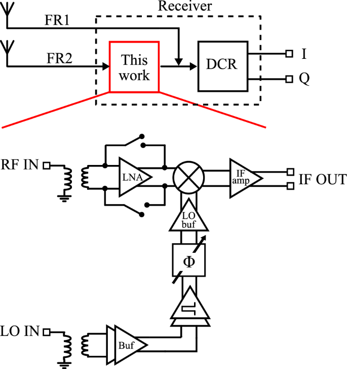
An 18–28 GHz dual-mode down-converter IC for 5G applications
Emerging spectrum trends require a higher integration of 5G New Radio Frequency Range 1 (FR1) and Frequency Range 2 (FR2) bands to enhance the availability of spectrum and spectrum-sharing opportunities. To enable the reception of both FR1 and FR2 bands in a seamless hardware entity, we propose combining homodyne and heterodyne architectures. This necessitates the incorporation of a down-converter module that transfers the incoming signals from FR2 bands down to FR1, ensuring compatibility with an FR1 direct-conversion receiver (DCR) for the final signal reception. The primary focus of this paper is the design and implementation of the required integrated down-converter. The module includes an integrated balun, a low-noise amplifier (LNA) with a bypass mode, a dual-mode mixer, and an intermediate frequency (IF) amplifier. The introduced bypass mode helps to further elevate the linearity performance compared to the nominal mode. The bypass mode is designed for joint communication and sensing operation to avoid the compression of the receiver. This work also incorporates a local oscillator (LO) signal distribution network with phase tuning elements using a mixed-signal approach. The circuit is implemented in a 22-nm CMOS process, and the active die area is 0.6 \(\text {mm}^\text {2}\). The measurements demonstrate that the implemented chip can efficiently perform the required frequency conversion over a wide frequency range of 18–28 GHz. Conversion gain of 4.5–7.5 dB, noise figure of 15–19.7 dB, 1 dB compression point (IP1dB) of − 16 to − 10 dBm, and input third-order intercept point (IIP3) of − 5 to 0 dBm are achieved. The measured IP1 dB and IIP3 for the bypass mode are +0.5 to +4.5 dBm and +8.5 to +10 dBm, respectively.
期刊介绍:
Analog Integrated Circuits and Signal Processing is an archival peer reviewed journal dedicated to the design and application of analog, radio frequency (RF), and mixed signal integrated circuits (ICs) as well as signal processing circuits and systems. It features both new research results and tutorial views and reflects the large volume of cutting-edge research activity in the worldwide field today.
A partial list of topics includes analog and mixed signal interface circuits and systems; analog and RFIC design; data converters; active-RC, switched-capacitor, and continuous-time integrated filters; mixed analog/digital VLSI systems; wireless radio transceivers; clock and data recovery circuits; and high speed optoelectronic circuits and systems.

 求助内容:
求助内容: 应助结果提醒方式:


