{"title":"在高真空中为铝接触 MoSe2 晶体管设计氧化钛夹层","authors":"Yoobin Oh, Youngho Jo, Woong Choi","doi":"10.1016/j.mee.2024.112139","DOIUrl":null,"url":null,"abstract":"<div><p>We present an enhanced performance of MoSe<sub>2</sub> transistors via sequentially depositing Ti and Al in high vacuum to establish TiO<sub>x</sub><span> interlayers positioned between the MoSe</span><sub>2</sub><span> channel and Ti/Al contacts. Transmission electron microscopy analysis revealed the presence of TiO</span><sub>x</sub> at the MoSe<sub>2</sub>/Ti interface. While MoSe<sub>2</sub> transistors exhibited poor device performance in the absence of a TiO<sub>x</sub> interlayer, the introduction of a TiO<sub>x</sub> interlayer yielded a notable transistor performance, including an on/off ratio of ∼10<sup>5</sup>, a field-effect mobility of ∼40 cm<sup>2</sup> V<sup>−1</sup> s<sup>−1</sup><span>, and a contact resistance of ∼100 kΩ μm. These enhancements were attributed to the beneficial effects of Fermi level unpinning and interfacial doping facilitated by TiO</span><sub>x</sub> interlayers. These results underscore the feasibility of incorporating TiO<sub>x</sub> interlayers to enable the use of conventional Al contacts in MoSe<sub>2</sub><span> transistors, delivering significant implications for enhancing the performance of transition metal dichalcogenide transistors.</span></p></div>","PeriodicalId":18557,"journal":{"name":"Microelectronic Engineering","volume":"286 ","pages":"Article 112139"},"PeriodicalIF":2.6000,"publicationDate":"2024-01-11","publicationTypes":"Journal Article","fieldsOfStudy":null,"isOpenAccess":false,"openAccessPdf":"","citationCount":"0","resultStr":"{\"title\":\"Engineering TiOx interlayers in high vacuum for Al-contacted MoSe2 transistors\",\"authors\":\"Yoobin Oh, Youngho Jo, Woong Choi\",\"doi\":\"10.1016/j.mee.2024.112139\",\"DOIUrl\":null,\"url\":null,\"abstract\":\"<div><p>We present an enhanced performance of MoSe<sub>2</sub> transistors via sequentially depositing Ti and Al in high vacuum to establish TiO<sub>x</sub><span> interlayers positioned between the MoSe</span><sub>2</sub><span> channel and Ti/Al contacts. Transmission electron microscopy analysis revealed the presence of TiO</span><sub>x</sub> at the MoSe<sub>2</sub>/Ti interface. While MoSe<sub>2</sub> transistors exhibited poor device performance in the absence of a TiO<sub>x</sub> interlayer, the introduction of a TiO<sub>x</sub> interlayer yielded a notable transistor performance, including an on/off ratio of ∼10<sup>5</sup>, a field-effect mobility of ∼40 cm<sup>2</sup> V<sup>−1</sup> s<sup>−1</sup><span>, and a contact resistance of ∼100 kΩ μm. These enhancements were attributed to the beneficial effects of Fermi level unpinning and interfacial doping facilitated by TiO</span><sub>x</sub> interlayers. These results underscore the feasibility of incorporating TiO<sub>x</sub> interlayers to enable the use of conventional Al contacts in MoSe<sub>2</sub><span> transistors, delivering significant implications for enhancing the performance of transition metal dichalcogenide transistors.</span></p></div>\",\"PeriodicalId\":18557,\"journal\":{\"name\":\"Microelectronic Engineering\",\"volume\":\"286 \",\"pages\":\"Article 112139\"},\"PeriodicalIF\":2.6000,\"publicationDate\":\"2024-01-11\",\"publicationTypes\":\"Journal Article\",\"fieldsOfStudy\":null,\"isOpenAccess\":false,\"openAccessPdf\":\"\",\"citationCount\":\"0\",\"resultStr\":null,\"platform\":\"Semanticscholar\",\"paperid\":null,\"PeriodicalName\":\"Microelectronic Engineering\",\"FirstCategoryId\":\"5\",\"ListUrlMain\":\"https://www.sciencedirect.com/science/article/pii/S016793172400008X\",\"RegionNum\":4,\"RegionCategory\":\"工程技术\",\"ArticlePicture\":[],\"TitleCN\":null,\"AbstractTextCN\":null,\"PMCID\":null,\"EPubDate\":\"\",\"PubModel\":\"\",\"JCR\":\"Q2\",\"JCRName\":\"ENGINEERING, ELECTRICAL & ELECTRONIC\",\"Score\":null,\"Total\":0}","platform":"Semanticscholar","paperid":null,"PeriodicalName":"Microelectronic Engineering","FirstCategoryId":"5","ListUrlMain":"https://www.sciencedirect.com/science/article/pii/S016793172400008X","RegionNum":4,"RegionCategory":"工程技术","ArticlePicture":[],"TitleCN":null,"AbstractTextCN":null,"PMCID":null,"EPubDate":"","PubModel":"","JCR":"Q2","JCRName":"ENGINEERING, ELECTRICAL & ELECTRONIC","Score":null,"Total":0}
Engineering TiOx interlayers in high vacuum for Al-contacted MoSe2 transistors
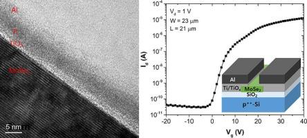
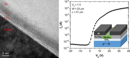
We present an enhanced performance of MoSe2 transistors via sequentially depositing Ti and Al in high vacuum to establish TiOx interlayers positioned between the MoSe2 channel and Ti/Al contacts. Transmission electron microscopy analysis revealed the presence of TiOx at the MoSe2/Ti interface. While MoSe2 transistors exhibited poor device performance in the absence of a TiOx interlayer, the introduction of a TiOx interlayer yielded a notable transistor performance, including an on/off ratio of ∼105, a field-effect mobility of ∼40 cm2 V−1 s−1, and a contact resistance of ∼100 kΩ μm. These enhancements were attributed to the beneficial effects of Fermi level unpinning and interfacial doping facilitated by TiOx interlayers. These results underscore the feasibility of incorporating TiOx interlayers to enable the use of conventional Al contacts in MoSe2 transistors, delivering significant implications for enhancing the performance of transition metal dichalcogenide transistors.
期刊介绍:
Microelectronic Engineering is the premier nanoprocessing, and nanotechnology journal focusing on fabrication of electronic, photonic, bioelectronic, electromechanic and fluidic devices and systems, and their applications in the broad areas of electronics, photonics, energy, life sciences, and environment. It covers also the expanding interdisciplinary field of "more than Moore" and "beyond Moore" integrated nanoelectronics / photonics and micro-/nano-/bio-systems. Through its unique mixture of peer-reviewed articles, reviews, accelerated publications, short and Technical notes, and the latest research news on key developments, Microelectronic Engineering provides comprehensive coverage of this exciting, interdisciplinary and dynamic new field for researchers in academia and professionals in industry.

 求助内容:
求助内容: 应助结果提醒方式:


