{"title":"采用 45 纳米 CMOS 技术为 PLL 应用设计 10 GHz 频率的高速 MCML 电荷泵","authors":"M. Sivasakthi, P. Radhika","doi":"10.1007/s10470-023-02225-0","DOIUrl":null,"url":null,"abstract":"<div><p>In this paper, a new high speed two-stage charge pump is designed for phase-locked loop (PLL) application. In the proposed circuit, switch-based charge pump acts as the primary charge pump for glitch-free output, in addition to that MOS current mode logic (MCML) based faster current driving charge pump acts as the secondary charge pump. It will used to achieve the PLL locking condition quickly. MCML circuits minimize delay and perform the fast operation, hence it can be used in high frequency applications. The proposed circuit achieves very low power of 13.19 μW with a minimum delay of 16.71 ps at 45 nm CMOS technology with a 1 V power supply in different process corners. The output noise as very low as − 232.7 dB and phase noise as − 247.2 dBc/Hz at 10 GHz frequency. The swing voltage ranges from 0 to 980 mV. Monte-Carlo simulations with 200 samples are analysed to verify the results. Finally, process voltage and temperature (PVT) analysis are performed to validate the stability of the proposed design. The simulated results shows that the proposed circuit is more stable for high-frequency PLL applications and is highly tolerant with PVT variations.</p></div>","PeriodicalId":7827,"journal":{"name":"Analog Integrated Circuits and Signal Processing","volume":"118 1","pages":"49 - 66"},"PeriodicalIF":1.2000,"publicationDate":"2023-12-29","publicationTypes":"Journal Article","fieldsOfStudy":null,"isOpenAccess":false,"openAccessPdf":"https://link.springer.com/content/pdf/10.1007/s10470-023-02225-0.pdf","citationCount":"0","resultStr":"{\"title\":\"A high-speed MCML charge pump design at 10 GHz frequency in 45 nm CMOS technology for PLL application\",\"authors\":\"M. Sivasakthi, P. Radhika\",\"doi\":\"10.1007/s10470-023-02225-0\",\"DOIUrl\":null,\"url\":null,\"abstract\":\"<div><p>In this paper, a new high speed two-stage charge pump is designed for phase-locked loop (PLL) application. In the proposed circuit, switch-based charge pump acts as the primary charge pump for glitch-free output, in addition to that MOS current mode logic (MCML) based faster current driving charge pump acts as the secondary charge pump. It will used to achieve the PLL locking condition quickly. MCML circuits minimize delay and perform the fast operation, hence it can be used in high frequency applications. The proposed circuit achieves very low power of 13.19 μW with a minimum delay of 16.71 ps at 45 nm CMOS technology with a 1 V power supply in different process corners. The output noise as very low as − 232.7 dB and phase noise as − 247.2 dBc/Hz at 10 GHz frequency. The swing voltage ranges from 0 to 980 mV. Monte-Carlo simulations with 200 samples are analysed to verify the results. Finally, process voltage and temperature (PVT) analysis are performed to validate the stability of the proposed design. The simulated results shows that the proposed circuit is more stable for high-frequency PLL applications and is highly tolerant with PVT variations.</p></div>\",\"PeriodicalId\":7827,\"journal\":{\"name\":\"Analog Integrated Circuits and Signal Processing\",\"volume\":\"118 1\",\"pages\":\"49 - 66\"},\"PeriodicalIF\":1.2000,\"publicationDate\":\"2023-12-29\",\"publicationTypes\":\"Journal Article\",\"fieldsOfStudy\":null,\"isOpenAccess\":false,\"openAccessPdf\":\"https://link.springer.com/content/pdf/10.1007/s10470-023-02225-0.pdf\",\"citationCount\":\"0\",\"resultStr\":null,\"platform\":\"Semanticscholar\",\"paperid\":null,\"PeriodicalName\":\"Analog Integrated Circuits and Signal Processing\",\"FirstCategoryId\":\"5\",\"ListUrlMain\":\"https://link.springer.com/article/10.1007/s10470-023-02225-0\",\"RegionNum\":4,\"RegionCategory\":\"工程技术\",\"ArticlePicture\":[],\"TitleCN\":null,\"AbstractTextCN\":null,\"PMCID\":null,\"EPubDate\":\"\",\"PubModel\":\"\",\"JCR\":\"Q4\",\"JCRName\":\"COMPUTER SCIENCE, HARDWARE & ARCHITECTURE\",\"Score\":null,\"Total\":0}","platform":"Semanticscholar","paperid":null,"PeriodicalName":"Analog Integrated Circuits and Signal Processing","FirstCategoryId":"5","ListUrlMain":"https://link.springer.com/article/10.1007/s10470-023-02225-0","RegionNum":4,"RegionCategory":"工程技术","ArticlePicture":[],"TitleCN":null,"AbstractTextCN":null,"PMCID":null,"EPubDate":"","PubModel":"","JCR":"Q4","JCRName":"COMPUTER SCIENCE, HARDWARE & ARCHITECTURE","Score":null,"Total":0}
A high-speed MCML charge pump design at 10 GHz frequency in 45 nm CMOS technology for PLL application
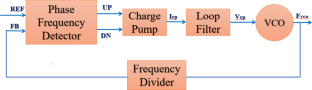
In this paper, a new high speed two-stage charge pump is designed for phase-locked loop (PLL) application. In the proposed circuit, switch-based charge pump acts as the primary charge pump for glitch-free output, in addition to that MOS current mode logic (MCML) based faster current driving charge pump acts as the secondary charge pump. It will used to achieve the PLL locking condition quickly. MCML circuits minimize delay and perform the fast operation, hence it can be used in high frequency applications. The proposed circuit achieves very low power of 13.19 μW with a minimum delay of 16.71 ps at 45 nm CMOS technology with a 1 V power supply in different process corners. The output noise as very low as − 232.7 dB and phase noise as − 247.2 dBc/Hz at 10 GHz frequency. The swing voltage ranges from 0 to 980 mV. Monte-Carlo simulations with 200 samples are analysed to verify the results. Finally, process voltage and temperature (PVT) analysis are performed to validate the stability of the proposed design. The simulated results shows that the proposed circuit is more stable for high-frequency PLL applications and is highly tolerant with PVT variations.
期刊介绍:
Analog Integrated Circuits and Signal Processing is an archival peer reviewed journal dedicated to the design and application of analog, radio frequency (RF), and mixed signal integrated circuits (ICs) as well as signal processing circuits and systems. It features both new research results and tutorial views and reflects the large volume of cutting-edge research activity in the worldwide field today.
A partial list of topics includes analog and mixed signal interface circuits and systems; analog and RFIC design; data converters; active-RC, switched-capacitor, and continuous-time integrated filters; mixed analog/digital VLSI systems; wireless radio transceivers; clock and data recovery circuits; and high speed optoelectronic circuits and systems.

 求助内容:
求助内容: 应助结果提醒方式:


