{"title":"1 - 5ghz 22mw接收器前端,主动反馈基带和电压换流混频器,65nm CMOS","authors":"Benqing Guo, Haishi Wang, Huifen Wang, Lei Li, Wanting Zhou, Kianoosh Jalali","doi":"10.1049/cds2.12124","DOIUrl":null,"url":null,"abstract":"<p>A CMOS baseband-active-feedback receiver frontend with passive voltage-commutating mixers is proposed. The active feedback baseband enables in-band signal amplification and out-of-band blocker interference suppression by constructing the RF bandpass filter and BB lowpass filter, simultaneously. The voltage-commutating mixers embedded in current mirrors significantly reduce the power requirement for the LO generator. The stacked n/pMOS structure is commonly adopted to further improve power efficiency. The receiver frontend is designed in a standard 65 nm CMOS process. Simulation results display an NF of 3.4 dB and a maximum gain of 32 dB from 1 to 5 GHz LO frequency range. The obtained in-band and out-of-band IIP3 are −12 dBm and 9 dBm, respectively. The receiver frontend core only consumes 22 mW at 1 GHz LO frequency and occupies the area of 645 × 543 μm<sup>2</sup>, which is suitable for the low-power application of handheld terminals.</p>","PeriodicalId":50386,"journal":{"name":"Iet Circuits Devices & Systems","volume":"16 7","pages":"543-552"},"PeriodicalIF":1.0000,"publicationDate":"2022-06-15","publicationTypes":"Journal Article","fieldsOfStudy":null,"isOpenAccess":false,"openAccessPdf":"https://ietresearch.onlinelibrary.wiley.com/doi/epdf/10.1049/cds2.12124","citationCount":"6","resultStr":"{\"title\":\"A 1–5 GHz 22 mW receiver frontend with active-feedback baseband and voltage-commutating mixers in 65 nm CMOS\",\"authors\":\"Benqing Guo, Haishi Wang, Huifen Wang, Lei Li, Wanting Zhou, Kianoosh Jalali\",\"doi\":\"10.1049/cds2.12124\",\"DOIUrl\":null,\"url\":null,\"abstract\":\"<p>A CMOS baseband-active-feedback receiver frontend with passive voltage-commutating mixers is proposed. The active feedback baseband enables in-band signal amplification and out-of-band blocker interference suppression by constructing the RF bandpass filter and BB lowpass filter, simultaneously. The voltage-commutating mixers embedded in current mirrors significantly reduce the power requirement for the LO generator. The stacked n/pMOS structure is commonly adopted to further improve power efficiency. The receiver frontend is designed in a standard 65 nm CMOS process. Simulation results display an NF of 3.4 dB and a maximum gain of 32 dB from 1 to 5 GHz LO frequency range. The obtained in-band and out-of-band IIP3 are −12 dBm and 9 dBm, respectively. The receiver frontend core only consumes 22 mW at 1 GHz LO frequency and occupies the area of 645 × 543 μm<sup>2</sup>, which is suitable for the low-power application of handheld terminals.</p>\",\"PeriodicalId\":50386,\"journal\":{\"name\":\"Iet Circuits Devices & Systems\",\"volume\":\"16 7\",\"pages\":\"543-552\"},\"PeriodicalIF\":1.0000,\"publicationDate\":\"2022-06-15\",\"publicationTypes\":\"Journal Article\",\"fieldsOfStudy\":null,\"isOpenAccess\":false,\"openAccessPdf\":\"https://ietresearch.onlinelibrary.wiley.com/doi/epdf/10.1049/cds2.12124\",\"citationCount\":\"6\",\"resultStr\":null,\"platform\":\"Semanticscholar\",\"paperid\":null,\"PeriodicalName\":\"Iet Circuits Devices & Systems\",\"FirstCategoryId\":\"5\",\"ListUrlMain\":\"https://onlinelibrary.wiley.com/doi/10.1049/cds2.12124\",\"RegionNum\":4,\"RegionCategory\":\"工程技术\",\"ArticlePicture\":[],\"TitleCN\":null,\"AbstractTextCN\":null,\"PMCID\":null,\"EPubDate\":\"\",\"PubModel\":\"\",\"JCR\":\"Q4\",\"JCRName\":\"ENGINEERING, ELECTRICAL & ELECTRONIC\",\"Score\":null,\"Total\":0}","platform":"Semanticscholar","paperid":null,"PeriodicalName":"Iet Circuits Devices & Systems","FirstCategoryId":"5","ListUrlMain":"https://onlinelibrary.wiley.com/doi/10.1049/cds2.12124","RegionNum":4,"RegionCategory":"工程技术","ArticlePicture":[],"TitleCN":null,"AbstractTextCN":null,"PMCID":null,"EPubDate":"","PubModel":"","JCR":"Q4","JCRName":"ENGINEERING, ELECTRICAL & ELECTRONIC","Score":null,"Total":0}
A 1–5 GHz 22 mW receiver frontend with active-feedback baseband and voltage-commutating mixers in 65 nm CMOS
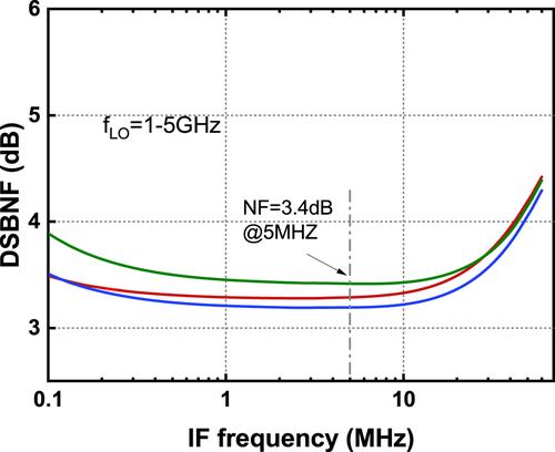
A CMOS baseband-active-feedback receiver frontend with passive voltage-commutating mixers is proposed. The active feedback baseband enables in-band signal amplification and out-of-band blocker interference suppression by constructing the RF bandpass filter and BB lowpass filter, simultaneously. The voltage-commutating mixers embedded in current mirrors significantly reduce the power requirement for the LO generator. The stacked n/pMOS structure is commonly adopted to further improve power efficiency. The receiver frontend is designed in a standard 65 nm CMOS process. Simulation results display an NF of 3.4 dB and a maximum gain of 32 dB from 1 to 5 GHz LO frequency range. The obtained in-band and out-of-band IIP3 are −12 dBm and 9 dBm, respectively. The receiver frontend core only consumes 22 mW at 1 GHz LO frequency and occupies the area of 645 × 543 μm2, which is suitable for the low-power application of handheld terminals.
期刊介绍:
IET Circuits, Devices & Systems covers the following topics:
Circuit theory and design, circuit analysis and simulation, computer aided design
Filters (analogue and switched capacitor)
Circuit implementations, cells and architectures for integration including VLSI
Testability, fault tolerant design, minimisation of circuits and CAD for VLSI
Novel or improved electronic devices for both traditional and emerging technologies including nanoelectronics and MEMs
Device and process characterisation, device parameter extraction schemes
Mathematics of circuits and systems theory
Test and measurement techniques involving electronic circuits, circuits for industrial applications, sensors and transducers
 求助内容:
求助内容: 应助结果提醒方式:


