{"title":"基于交错技术的低相位误差高指向性宽带180度可调谐有源耦合器的设计与分析","authors":"Samaneh Sadi, Abdolreza Nabavi, Massoud Dousti","doi":"10.1049/cds2.12131","DOIUrl":null,"url":null,"abstract":"<p>This study presents the design and analysis of a 180° tunable non-reciprocal active broadband coupler. To increase the bandwidth, the multi-section impedance transformation technique is utilised. The coupler includes two amplifiers, and three filters (phase-shifters) on the gate (drain) line, referred to as through-path (coupled-path). To achieve an accurate 180° broadband coupler, the staggering technique is utilised for designing the filters. Lumped-element analysis, adopted here for the first time to analyse the active coupler, reveals the impacts of each element on directivity, output phase-shift, and phase-error. The design and post-layout simulation of the coupler are performed in 0.18 µm CMOS technology over the frequency range of 10–20 GHz. An output phase of 180° ± 1.7°, a directivity more than 27 dB, and a return loss better than 10 dB are achieved. The coupling gain is 7.7 dB at the centre frequency, the noise figure is 4.8 dB, and the power consumption is 22 mW. By tuning the bias voltage, the phase imbalance caused by process variations can be compensated. Also, a prototype of the coupler was fabricated and tested on a Rogers substrate for 8–10 GHz band, giving an output phase of 180° ± 2° and a directivity >15 dB.</p>","PeriodicalId":50386,"journal":{"name":"Iet Circuits Devices & Systems","volume":"16 8","pages":"581-597"},"PeriodicalIF":1.0000,"publicationDate":"2022-10-31","publicationTypes":"Journal Article","fieldsOfStudy":null,"isOpenAccess":false,"openAccessPdf":"https://ietresearch.onlinelibrary.wiley.com/doi/epdf/10.1049/cds2.12131","citationCount":"1","resultStr":"{\"title\":\"Design and analysis of a tunable broadband 180-degree active coupler with low phase-error and high-directivity using staggering technique\",\"authors\":\"Samaneh Sadi, Abdolreza Nabavi, Massoud Dousti\",\"doi\":\"10.1049/cds2.12131\",\"DOIUrl\":null,\"url\":null,\"abstract\":\"<p>This study presents the design and analysis of a 180° tunable non-reciprocal active broadband coupler. To increase the bandwidth, the multi-section impedance transformation technique is utilised. The coupler includes two amplifiers, and three filters (phase-shifters) on the gate (drain) line, referred to as through-path (coupled-path). To achieve an accurate 180° broadband coupler, the staggering technique is utilised for designing the filters. Lumped-element analysis, adopted here for the first time to analyse the active coupler, reveals the impacts of each element on directivity, output phase-shift, and phase-error. The design and post-layout simulation of the coupler are performed in 0.18 µm CMOS technology over the frequency range of 10–20 GHz. An output phase of 180° ± 1.7°, a directivity more than 27 dB, and a return loss better than 10 dB are achieved. The coupling gain is 7.7 dB at the centre frequency, the noise figure is 4.8 dB, and the power consumption is 22 mW. By tuning the bias voltage, the phase imbalance caused by process variations can be compensated. Also, a prototype of the coupler was fabricated and tested on a Rogers substrate for 8–10 GHz band, giving an output phase of 180° ± 2° and a directivity >15 dB.</p>\",\"PeriodicalId\":50386,\"journal\":{\"name\":\"Iet Circuits Devices & Systems\",\"volume\":\"16 8\",\"pages\":\"581-597\"},\"PeriodicalIF\":1.0000,\"publicationDate\":\"2022-10-31\",\"publicationTypes\":\"Journal Article\",\"fieldsOfStudy\":null,\"isOpenAccess\":false,\"openAccessPdf\":\"https://ietresearch.onlinelibrary.wiley.com/doi/epdf/10.1049/cds2.12131\",\"citationCount\":\"1\",\"resultStr\":null,\"platform\":\"Semanticscholar\",\"paperid\":null,\"PeriodicalName\":\"Iet Circuits Devices & Systems\",\"FirstCategoryId\":\"5\",\"ListUrlMain\":\"https://onlinelibrary.wiley.com/doi/10.1049/cds2.12131\",\"RegionNum\":4,\"RegionCategory\":\"工程技术\",\"ArticlePicture\":[],\"TitleCN\":null,\"AbstractTextCN\":null,\"PMCID\":null,\"EPubDate\":\"\",\"PubModel\":\"\",\"JCR\":\"Q4\",\"JCRName\":\"ENGINEERING, ELECTRICAL & ELECTRONIC\",\"Score\":null,\"Total\":0}","platform":"Semanticscholar","paperid":null,"PeriodicalName":"Iet Circuits Devices & Systems","FirstCategoryId":"5","ListUrlMain":"https://onlinelibrary.wiley.com/doi/10.1049/cds2.12131","RegionNum":4,"RegionCategory":"工程技术","ArticlePicture":[],"TitleCN":null,"AbstractTextCN":null,"PMCID":null,"EPubDate":"","PubModel":"","JCR":"Q4","JCRName":"ENGINEERING, ELECTRICAL & ELECTRONIC","Score":null,"Total":0}
Design and analysis of a tunable broadband 180-degree active coupler with low phase-error and high-directivity using staggering technique
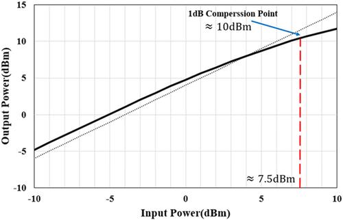
This study presents the design and analysis of a 180° tunable non-reciprocal active broadband coupler. To increase the bandwidth, the multi-section impedance transformation technique is utilised. The coupler includes two amplifiers, and three filters (phase-shifters) on the gate (drain) line, referred to as through-path (coupled-path). To achieve an accurate 180° broadband coupler, the staggering technique is utilised for designing the filters. Lumped-element analysis, adopted here for the first time to analyse the active coupler, reveals the impacts of each element on directivity, output phase-shift, and phase-error. The design and post-layout simulation of the coupler are performed in 0.18 µm CMOS technology over the frequency range of 10–20 GHz. An output phase of 180° ± 1.7°, a directivity more than 27 dB, and a return loss better than 10 dB are achieved. The coupling gain is 7.7 dB at the centre frequency, the noise figure is 4.8 dB, and the power consumption is 22 mW. By tuning the bias voltage, the phase imbalance caused by process variations can be compensated. Also, a prototype of the coupler was fabricated and tested on a Rogers substrate for 8–10 GHz band, giving an output phase of 180° ± 2° and a directivity >15 dB.
期刊介绍:
IET Circuits, Devices & Systems covers the following topics:
Circuit theory and design, circuit analysis and simulation, computer aided design
Filters (analogue and switched capacitor)
Circuit implementations, cells and architectures for integration including VLSI
Testability, fault tolerant design, minimisation of circuits and CAD for VLSI
Novel or improved electronic devices for both traditional and emerging technologies including nanoelectronics and MEMs
Device and process characterisation, device parameter extraction schemes
Mathematics of circuits and systems theory
Test and measurement techniques involving electronic circuits, circuits for industrial applications, sensors and transducers
 求助内容:
求助内容: 应助结果提醒方式:


