{"title":"1.2 kV低k介电介质中央栅极4H-SiC平面功率mosfet","authors":"Dong Liu, Mingyue Li, Yangjie Ou, Zhong Lan, Maosen Tang, Weibo Wang, Xiarong Hu","doi":"10.1049/cds2.12115","DOIUrl":null,"url":null,"abstract":"<p>A 1.2 kV 4H-SiC planar power MOSFET with a low-K dielectric in central gate (LK-MOS) is proposed in this paper. The LK-MOS features a P+ shielding region and a thick low-K dielectric layer under the central gate. The insulation layer capacitance is reduced by the thick low-K dielectric, while the depletion layer capacitance is decreased due to the reduced gate-to-drain overlap. The LK-MOS is demonstrated to have 97.8%, 70.6%, and 52.2% lower HF-FOM (<i>R</i><sub>on</sub> × <i>C</i><sub>gd</sub>), and 98.9%, 97.4%, and 69.4% lower HF-FOM (<i>R</i><sub>on</sub> × <i>Q</i><sub>gd</sub>), when compared with that of the conventional MOSFET (C-MOS), Buffered-Gate MOSFET (BG-MOS) and Thick Central Oxide MOSFET (TCOX-MOS), respectively. Besides, the LK-MOS can also have 16.8%, 5.9% lower <i>C</i><sub>gs</sub>, and 19.9%, 12.4% lower <i>Q</i><sub>gs</sub> compared with that of BG-MOS and TCOX-MOS.</p>","PeriodicalId":50386,"journal":{"name":"Iet Circuits Devices & Systems","volume":"16 5","pages":"419-426"},"PeriodicalIF":1.0000,"publicationDate":"2022-03-30","publicationTypes":"Journal Article","fieldsOfStudy":null,"isOpenAccess":false,"openAccessPdf":"https://ietresearch.onlinelibrary.wiley.com/doi/epdf/10.1049/cds2.12115","citationCount":"1","resultStr":"{\"title\":\"1.2 kV 4H-SiC planar power MOSFETs with a low-K dielectric in central gate\",\"authors\":\"Dong Liu, Mingyue Li, Yangjie Ou, Zhong Lan, Maosen Tang, Weibo Wang, Xiarong Hu\",\"doi\":\"10.1049/cds2.12115\",\"DOIUrl\":null,\"url\":null,\"abstract\":\"<p>A 1.2 kV 4H-SiC planar power MOSFET with a low-K dielectric in central gate (LK-MOS) is proposed in this paper. The LK-MOS features a P+ shielding region and a thick low-K dielectric layer under the central gate. The insulation layer capacitance is reduced by the thick low-K dielectric, while the depletion layer capacitance is decreased due to the reduced gate-to-drain overlap. The LK-MOS is demonstrated to have 97.8%, 70.6%, and 52.2% lower HF-FOM (<i>R</i><sub>on</sub> × <i>C</i><sub>gd</sub>), and 98.9%, 97.4%, and 69.4% lower HF-FOM (<i>R</i><sub>on</sub> × <i>Q</i><sub>gd</sub>), when compared with that of the conventional MOSFET (C-MOS), Buffered-Gate MOSFET (BG-MOS) and Thick Central Oxide MOSFET (TCOX-MOS), respectively. Besides, the LK-MOS can also have 16.8%, 5.9% lower <i>C</i><sub>gs</sub>, and 19.9%, 12.4% lower <i>Q</i><sub>gs</sub> compared with that of BG-MOS and TCOX-MOS.</p>\",\"PeriodicalId\":50386,\"journal\":{\"name\":\"Iet Circuits Devices & Systems\",\"volume\":\"16 5\",\"pages\":\"419-426\"},\"PeriodicalIF\":1.0000,\"publicationDate\":\"2022-03-30\",\"publicationTypes\":\"Journal Article\",\"fieldsOfStudy\":null,\"isOpenAccess\":false,\"openAccessPdf\":\"https://ietresearch.onlinelibrary.wiley.com/doi/epdf/10.1049/cds2.12115\",\"citationCount\":\"1\",\"resultStr\":null,\"platform\":\"Semanticscholar\",\"paperid\":null,\"PeriodicalName\":\"Iet Circuits Devices & Systems\",\"FirstCategoryId\":\"5\",\"ListUrlMain\":\"https://onlinelibrary.wiley.com/doi/10.1049/cds2.12115\",\"RegionNum\":4,\"RegionCategory\":\"工程技术\",\"ArticlePicture\":[],\"TitleCN\":null,\"AbstractTextCN\":null,\"PMCID\":null,\"EPubDate\":\"\",\"PubModel\":\"\",\"JCR\":\"Q4\",\"JCRName\":\"ENGINEERING, ELECTRICAL & ELECTRONIC\",\"Score\":null,\"Total\":0}","platform":"Semanticscholar","paperid":null,"PeriodicalName":"Iet Circuits Devices & Systems","FirstCategoryId":"5","ListUrlMain":"https://onlinelibrary.wiley.com/doi/10.1049/cds2.12115","RegionNum":4,"RegionCategory":"工程技术","ArticlePicture":[],"TitleCN":null,"AbstractTextCN":null,"PMCID":null,"EPubDate":"","PubModel":"","JCR":"Q4","JCRName":"ENGINEERING, ELECTRICAL & ELECTRONIC","Score":null,"Total":0}
1.2 kV 4H-SiC planar power MOSFETs with a low-K dielectric in central gate
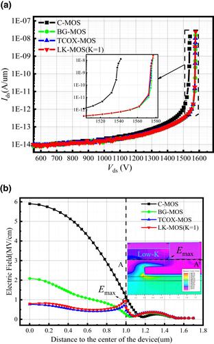
A 1.2 kV 4H-SiC planar power MOSFET with a low-K dielectric in central gate (LK-MOS) is proposed in this paper. The LK-MOS features a P+ shielding region and a thick low-K dielectric layer under the central gate. The insulation layer capacitance is reduced by the thick low-K dielectric, while the depletion layer capacitance is decreased due to the reduced gate-to-drain overlap. The LK-MOS is demonstrated to have 97.8%, 70.6%, and 52.2% lower HF-FOM (Ron × Cgd), and 98.9%, 97.4%, and 69.4% lower HF-FOM (Ron × Qgd), when compared with that of the conventional MOSFET (C-MOS), Buffered-Gate MOSFET (BG-MOS) and Thick Central Oxide MOSFET (TCOX-MOS), respectively. Besides, the LK-MOS can also have 16.8%, 5.9% lower Cgs, and 19.9%, 12.4% lower Qgs compared with that of BG-MOS and TCOX-MOS.
期刊介绍:
IET Circuits, Devices & Systems covers the following topics:
Circuit theory and design, circuit analysis and simulation, computer aided design
Filters (analogue and switched capacitor)
Circuit implementations, cells and architectures for integration including VLSI
Testability, fault tolerant design, minimisation of circuits and CAD for VLSI
Novel or improved electronic devices for both traditional and emerging technologies including nanoelectronics and MEMs
Device and process characterisation, device parameter extraction schemes
Mathematics of circuits and systems theory
Test and measurement techniques involving electronic circuits, circuits for industrial applications, sensors and transducers

 求助内容:
求助内容: 应助结果提醒方式:


