{"title":"5.5 - 7.5 ghz波段可配置唤醒接收器,完全集成在45nm RF-SOI CMOS中","authors":"Rui Ma, Florian Protze, Frank Ellinger","doi":"10.1049/cds2.12123","DOIUrl":null,"url":null,"abstract":"<p>This work investigates a 5.5–7.5-GHz band-configurable duty-cycled wake-up receiver (WuRX) fully implemented in a 45-nm radio-frequency (RF) silicon-on-insulator (SOI) complementary-metal-oxide-semiconductor (CMOS) technology. Based on an uncertain intermediate frequency (IF) super-heterodyne receiver (RX) topology, the WuRX analogue front-end (AFE) incorporates a 5.5–7.5-GHz band-tunable low-power low-noise amplifier, a low-power Gilbert mixer, a digitally controlled oscillator (DCO), a 100-MHz IF band-pass filter (BPF), an envelope detector, a comparator, a pulse generator and a current reference. By application of duty cycling with a low duty cycle below 1%, the power consumption of the AFE was significantly reduced. In addition, the on-chip digital bank-end consists of a frequency divider, a phase corrector, a 31-bit correlator and a serial peripheral interface. A proof-of-concept WuRX circuit occupying an area of 1200 <i>μ</i>m by 900 <i>μ</i>m has been fabricated in a GlobalFoundries 45-nm RF-SOI CMOS technology. Measurement results show that at a data rate of 64 bps, the entire WuRX consumes only 2.3 <i>μ</i>W. Tested at 8 operation bands covering 5.5–7.7 GHz, the WuRX has a measured sensitivity between −67.5 dBm and −72.4 dBm at a wake-up error rate of 10<sup>−3</sup>. With the sensitivity unchanged, the data rate of the WuRX can be scaled up to 8.2 kbps. To the authors' best knowledge, this work offers the largest RF bandwidth from 5.5 to 7.5 GHz, the most operation channels (≥8) and the fastest settling time (<115 ns) among the WuRXs reported to date.</p>","PeriodicalId":50386,"journal":{"name":"Iet Circuits Devices & Systems","volume":"16 7","pages":"525-542"},"PeriodicalIF":1.0000,"publicationDate":"2022-06-09","publicationTypes":"Journal Article","fieldsOfStudy":null,"isOpenAccess":false,"openAccessPdf":"https://ietresearch.onlinelibrary.wiley.com/doi/epdf/10.1049/cds2.12123","citationCount":"0","resultStr":"{\"title\":\"A 5.5–7.5-GHz band-configurable wake-up receiver fully integrated in 45-nm RF-SOI CMOS\",\"authors\":\"Rui Ma, Florian Protze, Frank Ellinger\",\"doi\":\"10.1049/cds2.12123\",\"DOIUrl\":null,\"url\":null,\"abstract\":\"<p>This work investigates a 5.5–7.5-GHz band-configurable duty-cycled wake-up receiver (WuRX) fully implemented in a 45-nm radio-frequency (RF) silicon-on-insulator (SOI) complementary-metal-oxide-semiconductor (CMOS) technology. Based on an uncertain intermediate frequency (IF) super-heterodyne receiver (RX) topology, the WuRX analogue front-end (AFE) incorporates a 5.5–7.5-GHz band-tunable low-power low-noise amplifier, a low-power Gilbert mixer, a digitally controlled oscillator (DCO), a 100-MHz IF band-pass filter (BPF), an envelope detector, a comparator, a pulse generator and a current reference. By application of duty cycling with a low duty cycle below 1%, the power consumption of the AFE was significantly reduced. In addition, the on-chip digital bank-end consists of a frequency divider, a phase corrector, a 31-bit correlator and a serial peripheral interface. A proof-of-concept WuRX circuit occupying an area of 1200 <i>μ</i>m by 900 <i>μ</i>m has been fabricated in a GlobalFoundries 45-nm RF-SOI CMOS technology. Measurement results show that at a data rate of 64 bps, the entire WuRX consumes only 2.3 <i>μ</i>W. Tested at 8 operation bands covering 5.5–7.7 GHz, the WuRX has a measured sensitivity between −67.5 dBm and −72.4 dBm at a wake-up error rate of 10<sup>−3</sup>. With the sensitivity unchanged, the data rate of the WuRX can be scaled up to 8.2 kbps. To the authors' best knowledge, this work offers the largest RF bandwidth from 5.5 to 7.5 GHz, the most operation channels (≥8) and the fastest settling time (<115 ns) among the WuRXs reported to date.</p>\",\"PeriodicalId\":50386,\"journal\":{\"name\":\"Iet Circuits Devices & Systems\",\"volume\":\"16 7\",\"pages\":\"525-542\"},\"PeriodicalIF\":1.0000,\"publicationDate\":\"2022-06-09\",\"publicationTypes\":\"Journal Article\",\"fieldsOfStudy\":null,\"isOpenAccess\":false,\"openAccessPdf\":\"https://ietresearch.onlinelibrary.wiley.com/doi/epdf/10.1049/cds2.12123\",\"citationCount\":\"0\",\"resultStr\":null,\"platform\":\"Semanticscholar\",\"paperid\":null,\"PeriodicalName\":\"Iet Circuits Devices & Systems\",\"FirstCategoryId\":\"5\",\"ListUrlMain\":\"https://onlinelibrary.wiley.com/doi/10.1049/cds2.12123\",\"RegionNum\":4,\"RegionCategory\":\"工程技术\",\"ArticlePicture\":[],\"TitleCN\":null,\"AbstractTextCN\":null,\"PMCID\":null,\"EPubDate\":\"\",\"PubModel\":\"\",\"JCR\":\"Q4\",\"JCRName\":\"ENGINEERING, ELECTRICAL & ELECTRONIC\",\"Score\":null,\"Total\":0}","platform":"Semanticscholar","paperid":null,"PeriodicalName":"Iet Circuits Devices & Systems","FirstCategoryId":"5","ListUrlMain":"https://onlinelibrary.wiley.com/doi/10.1049/cds2.12123","RegionNum":4,"RegionCategory":"工程技术","ArticlePicture":[],"TitleCN":null,"AbstractTextCN":null,"PMCID":null,"EPubDate":"","PubModel":"","JCR":"Q4","JCRName":"ENGINEERING, ELECTRICAL & ELECTRONIC","Score":null,"Total":0}
A 5.5–7.5-GHz band-configurable wake-up receiver fully integrated in 45-nm RF-SOI CMOS
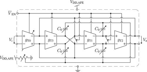
This work investigates a 5.5–7.5-GHz band-configurable duty-cycled wake-up receiver (WuRX) fully implemented in a 45-nm radio-frequency (RF) silicon-on-insulator (SOI) complementary-metal-oxide-semiconductor (CMOS) technology. Based on an uncertain intermediate frequency (IF) super-heterodyne receiver (RX) topology, the WuRX analogue front-end (AFE) incorporates a 5.5–7.5-GHz band-tunable low-power low-noise amplifier, a low-power Gilbert mixer, a digitally controlled oscillator (DCO), a 100-MHz IF band-pass filter (BPF), an envelope detector, a comparator, a pulse generator and a current reference. By application of duty cycling with a low duty cycle below 1%, the power consumption of the AFE was significantly reduced. In addition, the on-chip digital bank-end consists of a frequency divider, a phase corrector, a 31-bit correlator and a serial peripheral interface. A proof-of-concept WuRX circuit occupying an area of 1200 μm by 900 μm has been fabricated in a GlobalFoundries 45-nm RF-SOI CMOS technology. Measurement results show that at a data rate of 64 bps, the entire WuRX consumes only 2.3 μW. Tested at 8 operation bands covering 5.5–7.7 GHz, the WuRX has a measured sensitivity between −67.5 dBm and −72.4 dBm at a wake-up error rate of 10−3. With the sensitivity unchanged, the data rate of the WuRX can be scaled up to 8.2 kbps. To the authors' best knowledge, this work offers the largest RF bandwidth from 5.5 to 7.5 GHz, the most operation channels (≥8) and the fastest settling time (<115 ns) among the WuRXs reported to date.
期刊介绍:
IET Circuits, Devices & Systems covers the following topics:
Circuit theory and design, circuit analysis and simulation, computer aided design
Filters (analogue and switched capacitor)
Circuit implementations, cells and architectures for integration including VLSI
Testability, fault tolerant design, minimisation of circuits and CAD for VLSI
Novel or improved electronic devices for both traditional and emerging technologies including nanoelectronics and MEMs
Device and process characterisation, device parameter extraction schemes
Mathematics of circuits and systems theory
Test and measurement techniques involving electronic circuits, circuits for industrial applications, sensors and transducers
 求助内容:
求助内容: 应助结果提醒方式:


