Samira Shamsir, Laila Parvin Poly, Rajat Chakraborty, Samia Subrina
{"title":"石墨烯纳米带pn结和肖特基结二极管的电流-电压模型","authors":"Samira Shamsir, Laila Parvin Poly, Rajat Chakraborty, Samia Subrina","doi":"10.1049/cds2.12092","DOIUrl":null,"url":null,"abstract":"<p>This work presents a simplified analytical model of a p-n junction diode based on a graphene nanoribbon (GNR) and a unique type of Schottky diode based on metallic graphene and semi-conducting GNRs. Due to the one-dimensional nature of GNRs, their electrostatic analyses need to be quite different from that of bulk devices. Two approaches have been taken to model the charge distribution in this depletion region, namely, the point charge approximation for the GNR p-n junction diode and the line charge approximation for the graphene/GNR Schottky diode. Analytical expressions for the spatial distribution of electric field and potential have been derived and the results are quite distinct from their bulk counterparts. The current-voltage relation of each diode has been investigated within the approximation of Shockley's law of junctions. The width dependency of the currents for these diodes has also been modelled and it has been found that the current density of both the diodes decreases with decreasing width. Such an analysis can encourage the modelling of next-generation GNR-based high-speed electronic devices.</p>","PeriodicalId":50386,"journal":{"name":"Iet Circuits Devices & Systems","volume":"16 2","pages":"157-168"},"PeriodicalIF":1.0000,"publicationDate":"2021-07-30","publicationTypes":"Journal Article","fieldsOfStudy":null,"isOpenAccess":false,"openAccessPdf":"https://ietresearch.onlinelibrary.wiley.com/doi/epdf/10.1049/cds2.12092","citationCount":"4","resultStr":"{\"title\":\"Current-voltage model of a graphene nanoribbon p-n junction and Schottky junction diode\",\"authors\":\"Samira Shamsir, Laila Parvin Poly, Rajat Chakraborty, Samia Subrina\",\"doi\":\"10.1049/cds2.12092\",\"DOIUrl\":null,\"url\":null,\"abstract\":\"<p>This work presents a simplified analytical model of a p-n junction diode based on a graphene nanoribbon (GNR) and a unique type of Schottky diode based on metallic graphene and semi-conducting GNRs. Due to the one-dimensional nature of GNRs, their electrostatic analyses need to be quite different from that of bulk devices. Two approaches have been taken to model the charge distribution in this depletion region, namely, the point charge approximation for the GNR p-n junction diode and the line charge approximation for the graphene/GNR Schottky diode. Analytical expressions for the spatial distribution of electric field and potential have been derived and the results are quite distinct from their bulk counterparts. The current-voltage relation of each diode has been investigated within the approximation of Shockley's law of junctions. The width dependency of the currents for these diodes has also been modelled and it has been found that the current density of both the diodes decreases with decreasing width. Such an analysis can encourage the modelling of next-generation GNR-based high-speed electronic devices.</p>\",\"PeriodicalId\":50386,\"journal\":{\"name\":\"Iet Circuits Devices & Systems\",\"volume\":\"16 2\",\"pages\":\"157-168\"},\"PeriodicalIF\":1.0000,\"publicationDate\":\"2021-07-30\",\"publicationTypes\":\"Journal Article\",\"fieldsOfStudy\":null,\"isOpenAccess\":false,\"openAccessPdf\":\"https://ietresearch.onlinelibrary.wiley.com/doi/epdf/10.1049/cds2.12092\",\"citationCount\":\"4\",\"resultStr\":null,\"platform\":\"Semanticscholar\",\"paperid\":null,\"PeriodicalName\":\"Iet Circuits Devices & Systems\",\"FirstCategoryId\":\"5\",\"ListUrlMain\":\"https://onlinelibrary.wiley.com/doi/10.1049/cds2.12092\",\"RegionNum\":4,\"RegionCategory\":\"工程技术\",\"ArticlePicture\":[],\"TitleCN\":null,\"AbstractTextCN\":null,\"PMCID\":null,\"EPubDate\":\"\",\"PubModel\":\"\",\"JCR\":\"Q4\",\"JCRName\":\"ENGINEERING, ELECTRICAL & ELECTRONIC\",\"Score\":null,\"Total\":0}","platform":"Semanticscholar","paperid":null,"PeriodicalName":"Iet Circuits Devices & Systems","FirstCategoryId":"5","ListUrlMain":"https://onlinelibrary.wiley.com/doi/10.1049/cds2.12092","RegionNum":4,"RegionCategory":"工程技术","ArticlePicture":[],"TitleCN":null,"AbstractTextCN":null,"PMCID":null,"EPubDate":"","PubModel":"","JCR":"Q4","JCRName":"ENGINEERING, ELECTRICAL & ELECTRONIC","Score":null,"Total":0}
Current-voltage model of a graphene nanoribbon p-n junction and Schottky junction diode
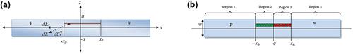
This work presents a simplified analytical model of a p-n junction diode based on a graphene nanoribbon (GNR) and a unique type of Schottky diode based on metallic graphene and semi-conducting GNRs. Due to the one-dimensional nature of GNRs, their electrostatic analyses need to be quite different from that of bulk devices. Two approaches have been taken to model the charge distribution in this depletion region, namely, the point charge approximation for the GNR p-n junction diode and the line charge approximation for the graphene/GNR Schottky diode. Analytical expressions for the spatial distribution of electric field and potential have been derived and the results are quite distinct from their bulk counterparts. The current-voltage relation of each diode has been investigated within the approximation of Shockley's law of junctions. The width dependency of the currents for these diodes has also been modelled and it has been found that the current density of both the diodes decreases with decreasing width. Such an analysis can encourage the modelling of next-generation GNR-based high-speed electronic devices.
期刊介绍:
IET Circuits, Devices & Systems covers the following topics:
Circuit theory and design, circuit analysis and simulation, computer aided design
Filters (analogue and switched capacitor)
Circuit implementations, cells and architectures for integration including VLSI
Testability, fault tolerant design, minimisation of circuits and CAD for VLSI
Novel or improved electronic devices for both traditional and emerging technologies including nanoelectronics and MEMs
Device and process characterisation, device parameter extraction schemes
Mathematics of circuits and systems theory
Test and measurement techniques involving electronic circuits, circuits for industrial applications, sensors and transducers
 求助内容:
求助内容: 应助结果提醒方式:


