Advanced approach of bulk (111) 3C-SiC epitaxial growth

IF 2.6 4区 工程技术 Q2 ENGINEERING, ELECTRICAL & ELECTRONIC
C. Calabretta , V. Scuderi , C. Bongiorno , R. Anzalone , R. Reitano , A. Cannizzaro , M. Mauceri , D. Crippa , S. Boninelli , F. La Via
{"title":"Advanced approach of bulk (111) 3C-SiC epitaxial growth","authors":"C. Calabretta ,&nbsp;V. Scuderi ,&nbsp;C. Bongiorno ,&nbsp;R. Anzalone ,&nbsp;R. Reitano ,&nbsp;A. Cannizzaro ,&nbsp;M. Mauceri ,&nbsp;D. Crippa ,&nbsp;S. Boninelli ,&nbsp;F. La Via","doi":"10.1016/j.mee.2023.112116","DOIUrl":null,"url":null,"abstract":"<div><p>3C-SiC films grown on (111) Si substrates exhibit poor crystal quality and experience wafer cracks and bowing preventing access to bulk growth. This work reports innovative Chemical Vapor Deposition (CVD) growth methodology on 4 in. Si substrates which allowed the growth of 230 mm thick layer of (111) 3C-SiC through the melting of the Si substrate in the CVD chamber and the adoption of the resulting free standing 3C-SiC for the growth of bulk (111) 3C-SiC layer under high N fluxes. From the molten KOH etching and subsequent SEM investigation it has been ascertained that with a N<sub>2</sub> flux of 1600 sccm there is a significant reduction in the concentration of stacking faults (SFs) from (7.16 ± 0.04) × 10<sup>3</sup> cm<sup>−1</sup> to (0.4 ± 0.3) × 10<sup>3</sup> cm<sup>−1</sup>. This reduction is consistent with the cross section m-PL response displaying steep and uniform increase in the intensity of the band-edge signal a factor 10 higher on the surface with respect to the equal (100) 3C-SiC grown thickness. Furthermore, the emission attributed to point defects is considerably lower in (111) 3C-SiC. From Scanning Transmission Electron Microscopy (STEM) investigation it appears evident how the typical mechanism valid in (100) growths consisting in the mutual closure of SFs coming from opposing {111} planes that give rise to Lomer and l-shaped dislocations is replaced by a different panorama of evolution. Indeed, it is shown how the SFs shred but do not interrupt each other during growth. Furthermore, dropping in the number of atomic planes composing SFs layers appears to be a key phenomenon leading to both the shrinkage of the number of SF atomic layers as well as to the SF self-closure. High Angle Annular Dark Field-Scanning Transmission Electron Microscopy (HAADF-STEM) attested how the crystal tends to smooth out the lattice mismatch until the SF is suppressed. Because of the foregoing, the mechanisms of evolution of the defects in (111) 3C-SiC revealed in this study, demonstrates how the growth parameters must be matched with the kinetics of the defects in order to endorse (111) 3C-SiC adoption in high performing devices.</p></div>","PeriodicalId":18557,"journal":{"name":"Microelectronic Engineering","volume":null,"pages":null},"PeriodicalIF":2.6000,"publicationDate":"2023-10-25","publicationTypes":"Journal Article","fieldsOfStudy":null,"isOpenAccess":false,"openAccessPdf":"https://www.sciencedirect.com/science/article/pii/S0167931723001818/pdfft?md5=db79438c2c09ef167cb61cb8c0cee2a3&pid=1-s2.0-S0167931723001818-main.pdf","citationCount":"0","resultStr":null,"platform":"Semanticscholar","paperid":null,"PeriodicalName":"Microelectronic Engineering","FirstCategoryId":"5","ListUrlMain":"https://www.sciencedirect.com/science/article/pii/S0167931723001818","RegionNum":4,"RegionCategory":"工程技术","ArticlePicture":[],"TitleCN":null,"AbstractTextCN":null,"PMCID":null,"EPubDate":"","PubModel":"","JCR":"Q2","JCRName":"ENGINEERING, ELECTRICAL & ELECTRONIC","Score":null,"Total":0}
引用次数: 0

Abstract

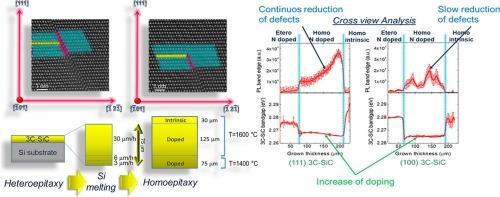
3C-SiC films grown on (111) Si substrates exhibit poor crystal quality and experience wafer cracks and bowing preventing access to bulk growth. This work reports innovative Chemical Vapor Deposition (CVD) growth methodology on 4 in. Si substrates which allowed the growth of 230 mm thick layer of (111) 3C-SiC through the melting of the Si substrate in the CVD chamber and the adoption of the resulting free standing 3C-SiC for the growth of bulk (111) 3C-SiC layer under high N fluxes. From the molten KOH etching and subsequent SEM investigation it has been ascertained that with a N2 flux of 1600 sccm there is a significant reduction in the concentration of stacking faults (SFs) from (7.16 ± 0.04) × 103 cm−1 to (0.4 ± 0.3) × 103 cm−1. This reduction is consistent with the cross section m-PL response displaying steep and uniform increase in the intensity of the band-edge signal a factor 10 higher on the surface with respect to the equal (100) 3C-SiC grown thickness. Furthermore, the emission attributed to point defects is considerably lower in (111) 3C-SiC. From Scanning Transmission Electron Microscopy (STEM) investigation it appears evident how the typical mechanism valid in (100) growths consisting in the mutual closure of SFs coming from opposing {111} planes that give rise to Lomer and l-shaped dislocations is replaced by a different panorama of evolution. Indeed, it is shown how the SFs shred but do not interrupt each other during growth. Furthermore, dropping in the number of atomic planes composing SFs layers appears to be a key phenomenon leading to both the shrinkage of the number of SF atomic layers as well as to the SF self-closure. High Angle Annular Dark Field-Scanning Transmission Electron Microscopy (HAADF-STEM) attested how the crystal tends to smooth out the lattice mismatch until the SF is suppressed. Because of the foregoing, the mechanisms of evolution of the defects in (111) 3C-SiC revealed in this study, demonstrates how the growth parameters must be matched with the kinetics of the defects in order to endorse (111) 3C-SiC adoption in high performing devices.
Abstract Image

块状(111)3C-SiC外延生长的先进方法
在(111)Si衬底上生长的3C-SiC薄膜表现出较差的晶体质量,并且经历晶圆裂纹和弯曲,阻碍了体生长。这项工作报告了创新的化学气相沉积(CVD)生长方法在4英寸。通过在CVD室中熔化Si衬底,并采用所得到的独立3C-SiC在高N通量下生长块状(111)3C-SiC层,Si衬底允许生长230 mm厚的(111)3C-SiC层。从熔融KOH蚀刻和随后的SEM研究中可以确定,当N2通量为1600 sccm时,层错(sf)的浓度从(7.16±0.04)× 103 cm−1显著降低到(0.4±0.3)× 103 cm−1。这种减小与横截面m-PL响应一致,显示出与等(100)3C-SiC生长厚度相比,表面上的带边信号强度急剧而均匀地增加了10倍。此外,在(111)3C-SiC中,由点缺陷引起的发射相当低。从扫描透射电子显微镜(STEM)的研究中可以明显看出,(100)生长中有效的典型机制是如何由来自相对{111}面的sf相互闭合组成的,从而产生洛默位错和l形位错,而这种机制是如何被不同的进化全景所取代的。事实上,它显示了SFs在生长过程中是如何分裂的,但并不相互中断。此外,原子面数量的减少似乎是导致原子层数量减少和自闭的关键现象。高角环形暗场扫描透射电子显微镜(HAADF-STEM)证明了晶体如何趋于平滑晶格不匹配,直到SF被抑制。由于上述原因,本研究揭示的(111)3C-SiC缺陷的演化机制表明,为了支持(111)3C-SiC在高性能器件中的应用,生长参数必须与缺陷动力学相匹配。
本文章由计算机程序翻译,如有差异,请以英文原文为准。
求助全文
约1分钟内获得全文 求助全文
来源期刊
Microelectronic Engineering
Microelectronic Engineering 工程技术-工程:电子与电气
CiteScore
5.30
自引率
4.30%
发文量
131
审稿时长
29 days
期刊介绍: Microelectronic Engineering is the premier nanoprocessing, and nanotechnology journal focusing on fabrication of electronic, photonic, bioelectronic, electromechanic and fluidic devices and systems, and their applications in the broad areas of electronics, photonics, energy, life sciences, and environment. It covers also the expanding interdisciplinary field of "more than Moore" and "beyond Moore" integrated nanoelectronics / photonics and micro-/nano-/bio-systems. Through its unique mixture of peer-reviewed articles, reviews, accelerated publications, short and Technical notes, and the latest research news on key developments, Microelectronic Engineering provides comprehensive coverage of this exciting, interdisciplinary and dynamic new field for researchers in academia and professionals in industry.
×
引用
GB/T 7714-2015
复制
MLA
复制
APA
复制
导出至
BibTeX EndNote RefMan NoteFirst NoteExpress
×
提示
您的信息不完整,为了账户安全,请先补充。
现在去补充
×
提示
您因"违规操作"
具体请查看互助需知
我知道了
×
提示
确定
请完成安全验证×
copy
已复制链接
快去分享给好友吧!
我知道了
右上角分享
点击右上角分享
0
联系我们:info@booksci.cn Book学术提供免费学术资源搜索服务,方便国内外学者检索中英文文献。致力于提供最便捷和优质的服务体验。 Copyright © 2023 布克学术 All rights reserved.
京ICP备2023020795号-1
ghs 京公网安备 11010802042870号
Book学术文献互助
Book学术文献互助群
群 号:481959085
Book学术官方微信